Table of Contents
Design files for this project can be found here (board + firmware), here (3D model).
Update 8/29/2021 – Added section for firmware written in Rust
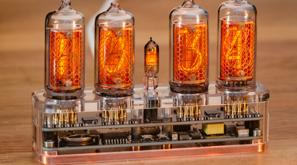
Ever since I started dabbling in electronics, I’ve wanted to build myself a Nixie tube clock completely from scratch. Building one isn’t easy though given the various barriers to entry: the high cost of Nixie tubes ($10-$50 each), high voltages for driving the tubes (~170V+), designing the PCB, the desire for an nice enclosure that isn’t 3D printed or made out of laser cut acrylic, etc. All together, it meant that I didn’t have the time, knowledge, or resources for this project until now.
In order to increase the probability that this project reaches completion, the feature list was kept as low as possible while still aiming for a working clock that I can build upon in future iterations. As such, the Nixie tubes themselves must be easy to source, which rules out expensive and/or rare tubes that are difficult to come by. The goal of this project is to create a basic clock, so only four digits are needed along with a digit separator. The power supply must be efficient, and should be powered off of USB-C if possible. Being a clock, RTC functionality along with the ability to keep time even when disconnected from power will naturally be required. Finally, the enclosure must be well designed, heavy, and preferably machined out of stainless steel, copper, or brass.


Common Nixie Tubes
Nixie tubes are available in effectively two orientations, side view (eg. IN-8/IN-14/IN-18) and end view (eg. IN-12/IN-17). A few good sites for comparing different tube models: Dieter’s Nixie World site has both side and end views from a variety of different manufacturers, Steampunk Alchemy’s site has pictures on soviet models and others, and Sphere Research’s Nixie Tube site has pictures on a large number of models as well. The neonixie-l google group is also an excellent resource with a large number of knowledgeable folks and active projects on it.
As I’m not a fan of open-source projects that uses rare components, the Nixie tubes for this project should be something that can be easily acquired. Soviet tubes looks to be widely available on eBay, and is thus a good choice since it’ll be cheaper and easier to replace parts. Non-soviet tubes are slightly more expensive for similar display sizes but have different digit shapes and better design/quality at the cost of being rarer. A quick comparison of common soviet tubes available on eBay (shipping adds +$10):
IN-17 — side mount, 9mm height, ~$4 each
IN-12 — side mount, 18mm height, ~$1.5 each (IN-12B has a left dot, IN12-A does not)
IN-14 — vertical mount, 18mm height, ~$4 each, long leads, has a fine grid version, pointed taper at the top
IN-8 — vertical mount, 18mm height, ~$10 each, flatter top compared to IN-14
IN-8-2 — same as IN-8 but with longer leads, has an alternate version with a much smaller grid
IN-18 — vertical mount, 40mm height, ~$50 each, huge but expensive
For a clock, you’ll also need a divider of some sort between the digits. Similar to Nixie tubes, there are neon bulbs that operate at a similar voltage with a similar color output. These bulbs are available in both side view (IN-3/IN-29) and end view (IN-6/IN-24/IN-28) variations. Neon bulbs are inexpensive compared to Nixie tubes due to their size, and can be found on Ebay in much larger quantities for cheap (10¢ for an IN-3). Note that TH4B/TH5B/MTH-90 models, while commonly advertised as Nixie tubes, are actually Thyratron tubes used for switching and rectifiers.


Preliminary Testing
For initial testing, a small high voltage power supply with a variable voltage output of 85-235V was used. The supply voltage was set at 170V and a 15k ohm resistor was used to limit the current to a safe level. The voltage drop measured across the resistor came out to be around ~37V, which corresponds to a ~133V drop across the tube and a drive current of ~2.5mA as the Nixie effectively short-circuits once the tube is ignited. The complete turn-off voltage was sightly lower than the voltage drop at ~124V. These values varied slightly between tubes, but not enough to really cause a difference in overall brightness. The ideal values for driving these tubes is unknown since the seller didn’t supply a datasheet. Most online resources list a voltage requirement of 170-200V with a cathode current of 2.0-3.5mA for IN-8 tubes, and 60-90V with a cathode current from 0.5-1.0mA for IN-3 bulbs.
The interesting observation here is that the tubes exhibits a large voltage drop while simultaneously acting as a short-circuit with regards to the current (almost exactly like a diode). When the tube was powered at 170V with all the digits off, the voltages at the cathode pins was measured to all be around ~44V. When I bumped the supply voltage to 200V, the voltages changed to ~74V. This happens to be very close to (supply voltage) – (turn off voltage). With a single digit turned on, the voltages on the other cathode pins varied depending on the distance of the measured digit to the one that is on. For the digit right next to the one on (physically, not numerically), the measured voltage came out to be exactly the same as the turn-off voltage. The further away the digit, the lower the voltage.


Driving Nixie Tubes
Most Nixie tube projects use vintage ICs 7441, 7441A, 74141, or the K155ID1 for driving the tubes. The 74141 and K155ID1 in particular are commonly used as a single IC is required per tube. They also have a built in BCD-to-decimal decoder, making it so that only 4 control lines were required to drive all digits of a given tube. These chips operate as current-sink drivers, sitting between the tube cathode pins and ground. The downside to using these chips is that they are relatively hard to find and only come in through hole DIP packages which takes up a significant amount of space on the PCB. Fine for most projects, but not ideal for the compact setup that I have in mind.
One alternative to these chips would be to use something similar to a shift register such as the HV5622. For my test setup, the driver would have to handle the turn-off voltage of ~124V (unless the supply voltage was more than double the turn-off voltage). The problem is that drivers capable of handling such high voltages via open collector or open drain outputs are rare, have large footprints, or are difficult to drive. I highly recommend EEVblog’s videos on searching for a suitable Nixie driver.
Voltage Clamping with Zener Diodes
Fortunately, there is a way to work around the high voltage requirement. By connecting a zener diode to each output of a lower voltage rated driver, the output voltage can be safely clamped (pre-biased) to a level that won’t damage the driver. The 74141 in fact uses zener diodes to clamp the output voltages at 55V. This results in a voltage drop of (supply voltage) – (zener clamp voltage) across the tube when the driver is off, which will be lower than the ignition/sustaining voltage if the clamp voltage is high enough. There are ICs that have this feature built in, such as the ULN2003 or the SN75468.
One possible issue to using zener diodes is that it changes the ‘current density’ inside the tube as a small amount of current is always drawn by each cathode. This results in an extra glowing ‘blue dots’ if the current density is too high as described quite well on this site. Details regarding this phenomenon is sparse, but it sounds like the issue can be avoided by clamping the output voltage to a higher level.
Switching with Transistors
There is a way to driving Nixie tubes without the use of zener diodes however, by opting for transistors that are capable of handling 200V or more. Modern bipolar transistors can easily meet this requirement while also being available in incredibly small packages: the MSD42WT1G at 10¢ each (quantities of 100+) is capable of switching up to 300V with a 2×2mm SOT-323 footprint. Combined with a logic level shift register, these BJT transistors can be configured as a simple switch to turn each digit of the tube on or off.
The downside to using this BJT and shift register combination is that it does not allow you to control the brightness of individual digits. This feature seems to be rare among other clock designs as most choose to dim the display by PWMing the anode supply. This works as a Nixie tube powered on behaves very much like an LED: to control the brightness of individual digits, the current or the PWM duty cycle for the each digit needs to be configurable.
Programmable Current Sink with BJTs
Similar to an LED, the brightness can be controlled by sinking a fixed current through each digit. One of the benefits of using a BJT transistor is that it can act as a fairly accurate current source in the right configuration. By varying the voltage at the base and placing a resistor between the emitter and ground, the collector current can be easily controlled. For example, a 1K ohm resistor and VB = 5V will result in VE = ~4.4V and IC = ~4.4mA regardless of VC. Given that VE and IC scales (mostly linearly) with VB, a few DACs with multiple outputs such as the BU2506FV can be used to set the current for each individual digit between 0 and ~4.4mA on a 5V rail. This method introduces a few new issues however, the first being that each transistor now dissipates a significant amount of power (0.2W at 40V/5mA) when on. Another issue is that Nixie tubes have a lower limit for the operating current; the digits have uneven brightness at low currents, and cease to be fully lit when a threshold of ~0.5mA is reached:


High Frequency Switching with BJTs
Again, similar to an LED, an alternative method for brightness control is to vary the on-period of each digit via a PWM signal. This can be done fairly easily by replacing the shift register with an IC that has configurable PWM outputs. One possible issue with this method of driving Nixie tubes in this fashion is that the display may exhibit visible flickering if the PWM frequency is low. Another possible issue with the PWM method is that the anode power supply may struggle to maintain a consistent voltage if the PWM period is synchronous (switching on/off at the same time) among all the drivers. If this happens, the supply current will rapidly alternate between zero and the desired current, which may result in extra instability from the boost supply switching between CCM and DCM modes.


One important difference between LEDs and Nixie tubes is that LEDs have near-instantaneous turn-on times while Nixie tubes have an inherent ignition delay. Because of this, there is a minimum on-time that must be met by the duty cycle. This is easily done by decreasing the modulation frequency, but comes at the cost of visible flickering. At higher frequencies, a longer duty cycle is needed to meet the minimum turn-on time, thus resulting in a higher minimum brightness. Ignition time is also reduced with higher anode voltages, potentially allowing for a lower minimum duty cycle.
Another important thing to take into consideration when choosing among the different method of driving Nixie tubes is the PCB footprint required for the driving circuitry. Discrete transistors will take up significantly more space compared to a single 74141, and even more so when additional ICs are required for driving the transistors. With a minimum of 40 transistors, 40 resistors, and a few ICs, the PCB becomes significantly more complex to route. There are ways to minimize the footprint however, by using resistor arrays and small footprint ICs.
Custom Driver PCB
After the initial testing was done, I went ahead and designed the first of two PCBs. The first PCB, the top half, contains only the components required for driving the Nixie tubes. Given the testing results, I opted to use discrete transistors and a few cascading PWM ICs to drive them. The PWM chips chosen was an expensive but feature-rich chip: the NXP PCA9685. With 12 bits per each of 16 outputs and an I2C interface, only three are needed to drive all 41 pins with some room to spare for future upgrades. There were three main features that I was looking for in the driver chip: 1) output driver capability, 2) large operating voltage range, and 3) ability to phase shift each output.
The PCA9685 fits the bill perfectly as the outputs can be configured as open drain or totem pole (most PWM chips for driving LEDs are open drain only). It also has an operating voltage range of 2.3V to 5.5V, so by changing the supply voltage, the baseline current is programmable from ~1.7mA to ~4.9mA. Finally, the delay between the rising edge of each output can be individually configured. With a bit of extra logic, the current consumption of the tubes can be load balanced to maintain a more consistent load on the power supply. By adjusting the phase of each output such that the ‘on’ period has minimal overlap, the peak current can be reduced by up to 75% compared to a driver with non-phase shifted outputs. This amount of savings only happens when the duty cycle is less than 25%, but otherwise it scales somewhat linearly to the point of maximum peak current at 100% duty cycle.
The other half of driving the outputs is the high voltage transistors. I opted to use discrete high voltage NPN transistors here: the ON MSD42WT1G. The main feature of this transistor is it’s voltage rating: with a maximum VCE and VCB rating of 300V, there is an additional 50% buffer for voltage transients. It also comes in one of the smallest SMD footprints available for transistors, the SOT-323. This is quite important due to the number of transistors needed. The other parameters are nice as well, with VBE of 6V being higher than the operating voltage of the PWM chips along and the capability to continuously handle up to 3mA at VCE of 200V.
Rev. A PCB Layout
A significant amount of effort was put into routing the board to make the PCB as small as possible while only using two copper layers to keep the cost down. Routing a four layer board would have made things easier, but would have also doubled the cost. The resulting 20mm × 100mm PCB is just slightly larger than the bounding box of the tubes themselves when placed side by side. High and low voltage traces were also isolated as much as possible give the physical constraints of the board. High voltage traces (right input) are primarily routed on the top layer while logic level traces (left input) are routed on the bottom layer with both circuits having isolated grounds. Two holes for M2.5 screws were also placed in the middle for structural support using standoffs between the boards.


Rev. B PCB Layout
There were a few issues that I wanted to address with the second revision of the driver board:
- No ground shielding plane between the high voltage switching signals and the logic level signals.
- Corners of the PCB needs to be rounded due to enclosure manufacturing requirements.
- High voltage and logic grounds should be merged as the same ground reference is used by the driver (for current control) and by the Nixie tubes (cathode reference).
- More structural rigidity from the signal/power headers.
To address these concerns while keeping the overall board dimensions the same, I had to re-design the board using four layers. The top layer is mainly used for components and high voltage switching traces. The following layer is mainly used as a ground and power plane. The bottom two layers are used for signal traces. The two additional layers in this revision both decreased trace routing complexity as well as added space for new features in the future.


Bill of Materials
| Count | Description | Footprint | Part Number |
| 41 | Transistor – NPN, 300V, 150mA | SOT-323 | MSD42WT1GOSCT-ND |
| 40 | Resistor – 1kΩ, 1/10W, 1% | 0603 | 311-1.00KHRCT-ND |
| 1 | Resistor – 3.9kΩ, 1/10W, 1% | 0603 | 311-3.90KHRCT-ND |
| 3 | Capacitor – 1μF, X7R | 0603 | 1276-6613-1-ND |
| 40 | Sockets – 1mm | 1.5mm | Ebay or Harwin |
| 3 | IC – PWM Controller, PCA9685 | QFN-28 | 568-5305-1-ND |
| 1 | Header – Two Terminal Spring Cage | 5.5mm × 5.0mm | 277-2086-1-ND |
| 2 | Header – Harwin Datamate L-Tek, Male | 5.6mm × 9.5mm | 952-1882-ND |
HV Power Supply
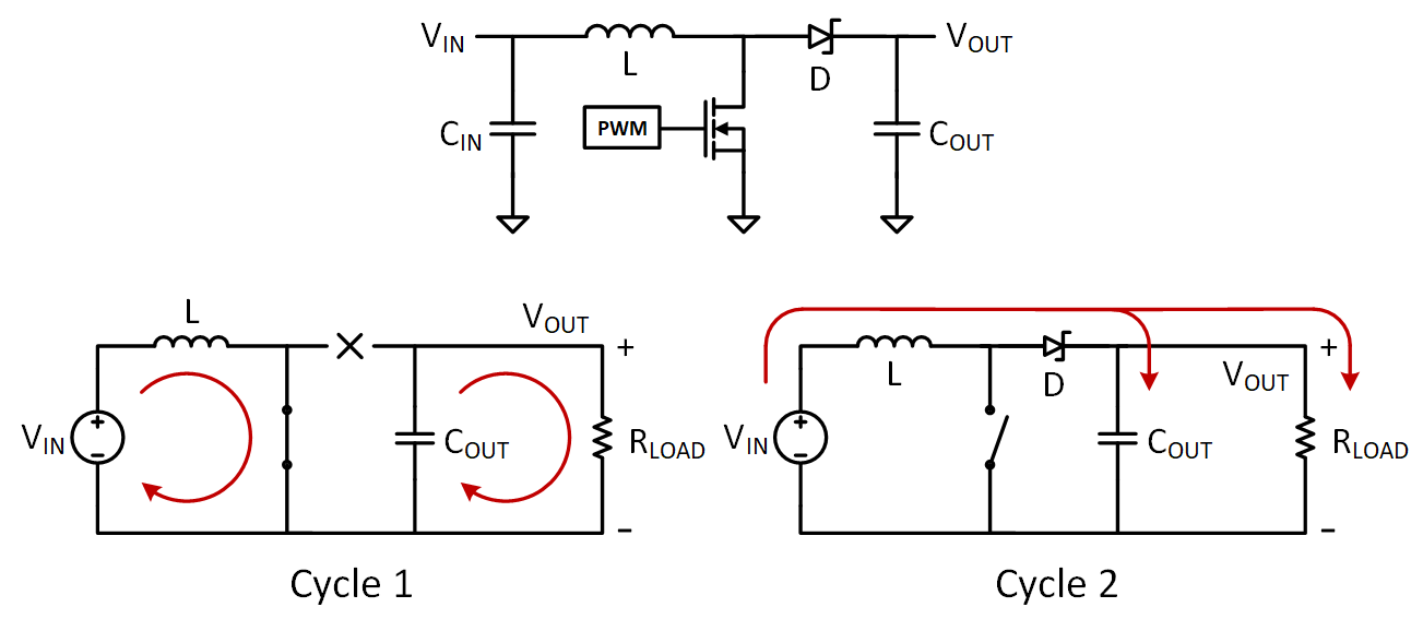
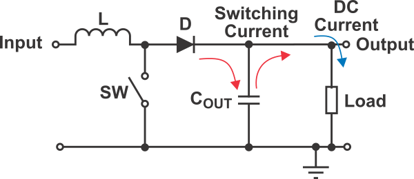
The other half to driving Nixie tubes involves the high voltage power supply. A high efficiency DC-DC boost converter circuit is commonly used in Nixie tube projects to generate such high voltages. There are two variations of this converter circuit: one uses a inductor (boost) while the other uses a transformer choke (flyback). Each has its own merits: inductors are usually available in larger selection of both value and footprints while transformer can utilize a winding ratio to reduce the peak current and voltage load on both the inductor and switch.
If you are looking for a good off-the-shelf power supply, YanZeyuan’s NCH6100HV is a pretty good choice. As a word of warning, don’t get the cheaper knockoffs as they use inferior components. The fake one I got was capable of sourcing ~200V but could only source 8mA compared to the 40mA from a genuine NCH6100HV. The NCH8200HV is also a good choice if you are looking for a smaller high efficiency (86% @ 17mm × 18mm) power supply. Another example of a flyback design with minimal footprint for boosting 5V to 170V can be found here.
Power Supply Design
Rather than buying a commercial unit and integrating it into my project, I wanted to get some experience with the process of designing a power supply from scratch. The section below details the results of my investigations into power supply design as well as to provide a guide for those looking to build one of their own.
There are a number of excellent resources on the design and operation of boost converters, the foremost being the books Art of Electronics, Switching Power Supply Design, and Switchmode Power Supply Handbook. For web-based resources, this site covers the basics while these TI app notes go into more detail. This project page details the design of a custom high voltage boost converter, while this one does a good job at explaining how to optimize component placement on the PCB. There are similar articles and resources detailing the differences between boost and flyback circuits.
Disclaimer: while many of the equations below for boost components were directly copied from various app notes, most of the equations for flyback components were manually derived due to lack of references. See this page for more info.
SMPS Fundamentals: CCM vs DCM
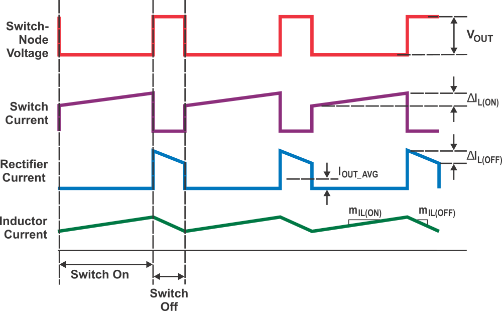
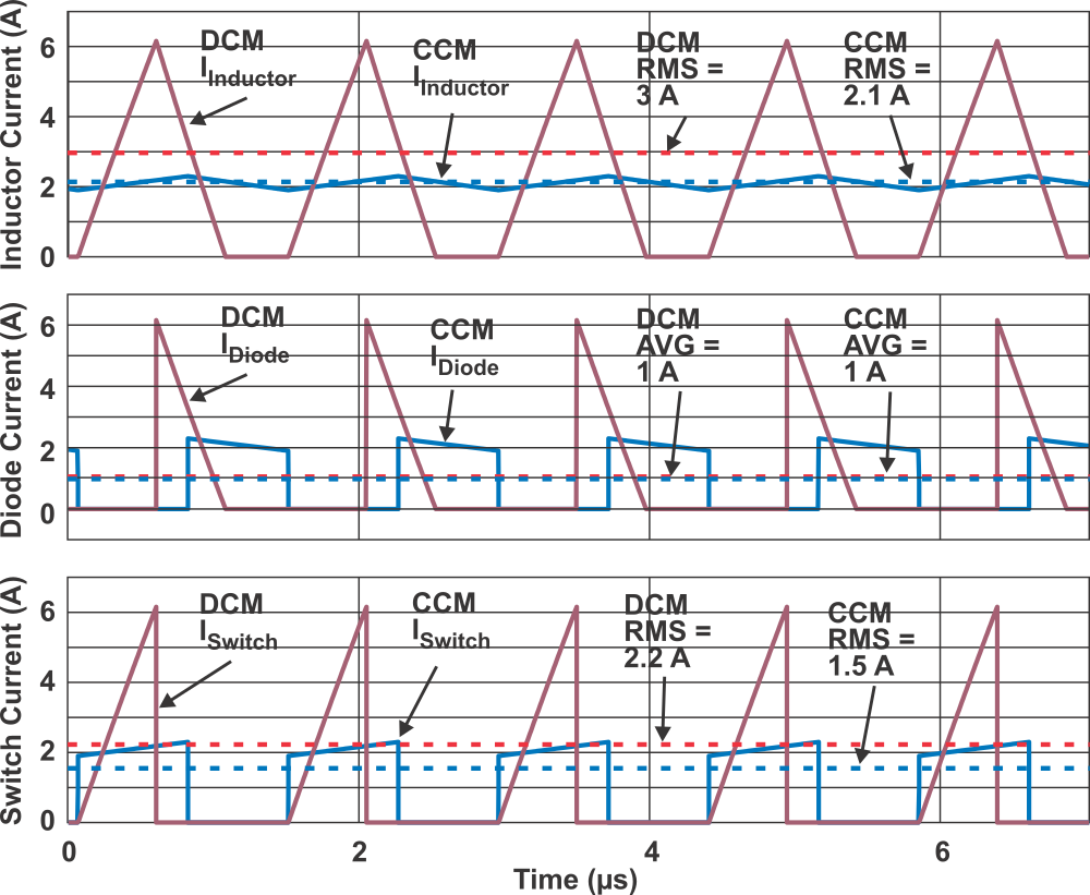
There are two fundamentally different operating modes for both boost and flyback converters. The first, continuous-conduction mode (CCM), occurs when the current in the inductor continues flowing during all stages of operation. The energy stored in the inductor increases while the switch is on and is equal to the energy discharged into the load through the diode when the switch is off, thereby ensuring steady-state operation. Because the current in the inductor never reaches zero, residual energy remains in the inductor at the end of each switching cycle.
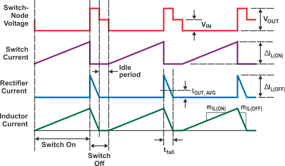
In discontinuous-conduction mode (DCM), the energy stored in the inductor when the switch is on is equal to the energy required by the load for one switching cycle. The energy stored in the inductor is depleted to zero when the switch is turned off, and results in a period where there is no current flowing through the inductor. This results in higher peak currents through the components as well as a larger ripple voltage at the output of the converter. The benefit of DCM operation is the lower inductance requirement which can lead to a smaller footprint for the inductor.
Selecting a mode of operation is essential in the design of a boost converter as it impacts both the component choice as well as the resulting performance and efficiency of the converter when operating under design constraints. Efficiency is lower in DCM mode as peak currents are higher (due to the faster/complete discharge of the inductor) through the components. Maintaining operation in CCM mode requires a minimum load current however, which may not be achievable if PWM is used to control the brightness of the Nixie tubes.
Designing a converter that operates in CCM mode is also more difficult due to issues such as sub-harmonic instability and transitions between DCM (startup) and CCM (steady-state). Details of such issues are left out of this writeup, but can be found in resources listed at the start of this section.
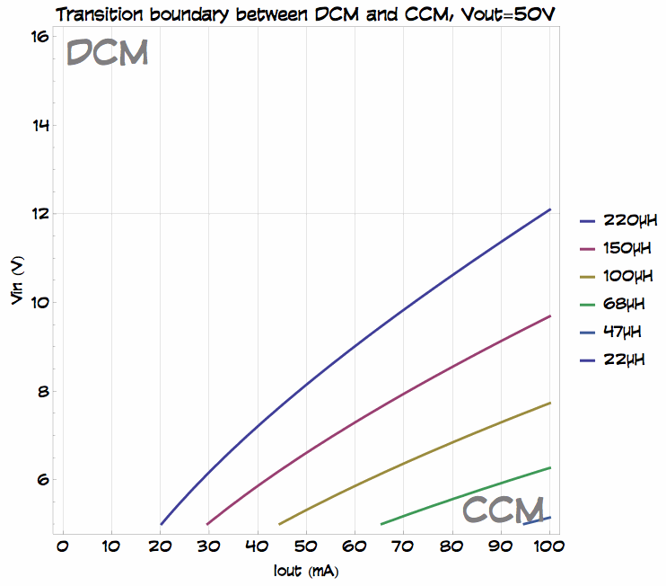
Since I’m planning on utilizing PWM for brightness control with a focus on minimizing the overall footprint, designing my power supply to operate solely in DCM seems to be ideal. For both types of circuits, the duty cycle boundary between CCM and DCM should first be computed:


Where VD is the voltage drop across the rectifier diode and Ns:p is the secondary:primary turn ratio for the transformer. The small difference in duty cycle when N=1 is due to the minimum voltage across the inductor: in a boost circuit, the voltage drops to Vin while the voltage across the secondary winding of a flyback’s transformer drops to zero. To compute the boundary value for the inductance required for CCM or DCM:
 and
and 
Where FS is the switching frequency. As depicted in the graphs above, the converter will operate in DCM if the inductance is kept below the the boundary value.
While the operating duty cycle (inductor charging/discharging) in CCM is dependent solely on the input and output voltages, the same does not apply in DCM as there is a period where the inductor is completely discharged. Furthermore, in DCM, the duty cycle varies more with load changes than it does when running in CCM. Many boost controllers have both a maximum and minimum switching frequency so care must be taken to keep the operating duty cycle within the capabilities of the boost controller. The DCM duty cycle can be computed by taking the inductance and switching frequency into account:
 and
and 
Ddcm here is the duty cycle at the given switching frequency when the switch is on (inductor is charging). The duty cycle for the discharge period can be found with:
 and
and 
The time in which the inductor is active is  , and should be taken into consideration when choosing the switching frequency. Leaving an additional 20% buffer is recommended to ensure that the circuit operates in DCM.
Inductor/Transformer

There are two main considerations that should be taken when choosing an inductor for a boost converter: the inductance and maximum current rating. Additional considerations include the winding resistance, shielding, core material, and size. For transformers, the turn ratio and the leakage inductance should also be taken into account. The (primary) inductance value needs to be less than the CCM threshold in order to maintain DCM at the desired load.
The maximum current rating is also important as the peak current through the inductor will be significant higher than the average load current. The peak current in the inductor or primary winding of a transformer can be computed as follows:
 (in DCM only)
Where L is the inductance of the primary coil of the transformer for a flyback circuit and  . Due to this high ripple current, when selecting an inductor, a core material with low permeability and low core losses at the switching frequency should be chosen to minimize power dissipation. A shielded inductor will result in less RFI but will also slightly lower the overall efficiency. Care should also be taken to ensure that the peak current does not exceed the saturation current rating of the inductor or transformer. Conduction losses in the inductor for a boost circuit can be approximated with:
 where
where  (boost topology, in DCM only)
For flyback circuits, conduction losses are calculated separately for the primary and secondary windings:
 (flyback topology, in DCM only)
MOSFET Switch
There are four important parameters when selecting a MOSFET switch: VDS (drain-source breakdown voltage), RDS(on) (drain-source on resistance), Qg (gate charge), and Coss (output capacitance). The breakdown voltage VDS should be greater than or equal to 1.5x the expected voltage across the switch. For a boost circuit, VDS(max) = Vout. For a flyback circuit, VDS(max) = Vin + Vclamp where Vclamp is the clamp circuit voltage. Design guidelines for snubber and clamp circuits is provided later in this section.
Power dissipation of the switch is comprised of gate, conduction, and switching losses. The gate losses can be approximated using the gate capacitance, gate voltage and switching frequency:

The on-resistance of the switch, RDS, is used to approximate the conduction losses:
 where
where  and
and  (in DCM only)
Switching losses originate from having to charge and discharge the node capacitances (Coss and Crss) along with losses during the transition periods from the Miller effect at low gate voltages:

![\dfrac{I_{out}\times N_{s:p}}{D_{dis}}\times\dfrac{Q_{gd}\times R_G}{V_G-V_{G(th)}}\bigg]](https://0x7d.com/wp-content/ql-cache/quicklatex.com-b87f66d1cdbe69283955fbdee4f291e9_l3.png "Rendered by QuickLaTeX.com") (in DCM only)
(in DCM only)
Where N is 1 for an inductor (boost circuit). For a more through explanation regarding power losses in switching MOSFETs, reference these app notes. Note that the switching losses needs to be doubled as there are two charge/discharge cycles per switching period.
Rectifier Diode
The output rectifier diode must be capable of handling the peak reverse voltage, peak input current, and the diode’s average power. In a boost circuit,  . In a flyback circuit,
  . A simple approximation of conduction losses in the diode is:
 where
where  and
and  (in DCM only)
For lower output voltages, a low capacitance Schottky diode is recommended. For higher output voltages, a fast recovery diode should be chosen. Soft recovery characteristics, normally desirable when operating in CCM, are not required when operating in DCM as there is no current flowing through the diode when the switch is on. Switching losses associated with a Schottky diode is based off the diode’s capacitance while the losses when using a fast-recovery diode is determined by the recovery time:
 and
and  (in DCM only)
For higher efficiency in low-current applications with high output currents or low output voltages, it is often advantageous to implement synchronous rectification with a second MOSFET in place of the diode. This adds additional implementation complexity, but greatly increases efficiency as the voltage drop across the rectifier diode is effectively negated. Some controllers even have built-in support for a synchronous MOSFET. Reference this TI app note for more information.
Synchronous rectification with a MOSFET does not really work with high output voltages however. The reason for this is because the gate-source voltage of the MOSFET needs to be higher than peak output voltage in order to turn the MOSFET on. Needless to say, generating a gate voltage higher than the output voltage is quite tricky to do.
Input/Output Capacitors
Capacitors are required in order to limit the voltage ripple at both the input and output. In a flyback topology, the input current is discontinuous so more capacitance is typically needed. Capacitor selection is critical for proper operation: ceramic capacitors (with negligible ESR) are typically chosen to limit the amount of ripple voltage while aluminum electrolytic/polymer or tantalum capacitors are typically used to add bulk capacitance to prevent large voltage swings when switching high loads. In both cases, the ripple current rating of the capacitor must be greater than IS(rms) (input) or ID(rms) (output).
The voltage drop across the capacitor can be computed as a function of the current, capacitance, and time:  . Assuming a steady-state load current, the minimum capacitance and maximum ESR of the input capacitor to maintain a given voltage ripple at the input can be estimated as follows:
 and
and  (in DCM only)
The output capacitor is used to reduce the ripple voltage at the output. The minimum capacitance and maximum ESR of the capacitor to maintain a given voltage ripple at the output can be estimated as follows:
 and
and  (in DCM only)
Power dissipation of the output capacitor can be computed using the current and capacitor’s ESR:
 where
where  (in DCM only)
Snubber and Clamp Circuits
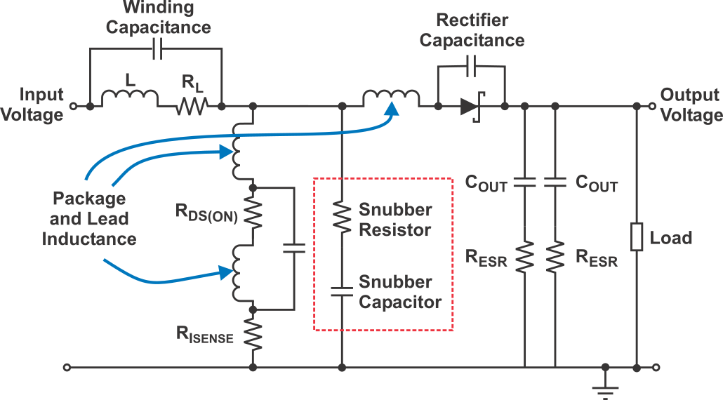
In addition to the main components listed above, some additional parts are needed to ensure stability in various parts of the circuit. Parasitic components such as inductor shunt capacitance and lead-wire inductance in the MOSFET and diode can cause ringing at the switch node in excess of 100Mhz. This ringing generate EMI and will damage the MOSFET if the ringing voltage peak is too high.
To address this issue, a RC snubber can be added in parallel to the MOSFET to dampen the parasitic energy. Methods to optimize the RC values is described in these app notes. The initial RC values can be estimated with:
 and
and 
Where tr is the desired rise time at the switch node and VC(max) is the maximum voltage across the MOSFET. The power dissipation of the snubber resistor can be approximated with:

This ringing is especially problematic in flyback transformers due to the leakage inductance between the transformer windings. The leakage energy resulting from the leakage inductance is kept in the primary winding when the switch is turned off, resulting in a large voltage spike at the MOSFET’s drain terminal.
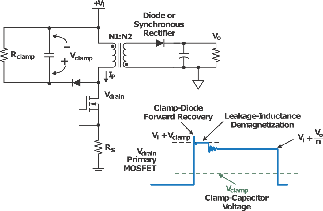
To protect the MOSFET from this voltage spike, a RCD clamp circuit should be added in parallel across the primary winding of the transformer to create a low impedance voltage source. This circuit clamps to a voltage that is usually 2x higher than the reflected output voltage (Vout/Ns:p) to keep the voltage across the MOSFET within an acceptable range. A higher clamp voltage decreases the switching time (and thus losses), but increases EMI and MOSFET drain voltage.
This voltage is relatively constant during a switching cycle and reaches its maximum value when powering a full load with minimum input voltage:
 and
and 
Where Lleak is the leakage inductance on the primary winding, Ipk is the peak current on the primary winding, Vclamp is the desired voltage to clamp the MOSFET’s drain to, and Vclamp(ripple) is the voltage ripple across Cclamp (5-10% of Vclamp). The diode should have a fast forward recovery time to reduce the voltage spike as well as being able to handle Ipk with a reverse voltage rating greater than Vclamp + Vin. The power dissipation of the clamp circuit can be approximated with:

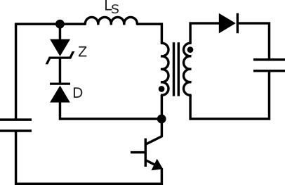
An alternative to the RCD clamp is the DZ (diode-Zener) clamp. Schottky diodes are typically the better choice here due to their faster turn-on time. Similar to the RCD clamp, the diode needs to be able to handle Ipk and have a reverse voltage greater than Vclamp + Vin where Vclamp is set by the Zener reverse breakdown voltage. The power loss in the clamp circuit determines the required power rating of the Zener diode. Power loss is highest maximum load and minimum input voltage. A higher Zener breakdown voltage will reduce the power loss but the breakdown voltage rating must be below the MOSFET’s voltage rating (VDS(max) – Vin) with some margin.
![P_{clamp}=\dfrac{1}{2}\times L_{leak}\times I_{pk}^2\times F_S\times \bigg[1+\dfrac{V_{out}+V_F}{N_{s:p}\times V_{zener}-(V_{out}+V_F)}\bigg]](https://0x7d.com/wp-content/ql-cache/quicklatex.com-c45a443a4903b5c39928dfca19b0065c_l3.png "Rendered by QuickLaTeX.com")
Where Vzener is the Zener diode breakdown voltage, VF is the voltage drop across the clamp diode and VD is the voltage drop across the output rectifier diode. The DZ clamp should have slightly higher efficiency compard to the RCD clamp circuit at the cost of higher EMI.
While a clamp circuit is typically required, omitting the clamp or snubber is possible if the peak voltage resulting from the transformer’s leakage inductance is lower than the switching MOSFET’s voltage rating. This is best determined by empirical means, but can also be estimated with:

Where Vpk is the peak voltage seen at the drain of the MOSFET, Lleak(pri) is the primary leakage inductance, CL is the transformer capacitance on the primary winding, and Coss is the output capacitance of the MOSFET. The leakage inductance on the secondary winding also results in some ringing when coupled with the reverse recovery current of the output rectifier diode. This overshoot may result in significant EMI as well as possibly exceeding the rectifier diode’s voltage rating. The voltage peak on the secondary can be estimated with:

Where Irev is the reverse recovery current, Lleak(sec) is the leakage inductance on the secondary winding, and CD is the rectifier diode’s capacitance. Additional margin should also be added to the peak values to account for parasitics.
SMPS Controller IC
Last but not least, there is the controller which contains the logic and circuitry for driving the MOSFET and regulating the duty cycle and/or switching frequency to maintain the desired output voltage at any given load. These controller ICs can range from simple 555 timers to feature-rich integrated controllers such as the MAX1771, TPS40210, or LT8304. There are many more controller available from a variety of vendors for DC-DC converters with various features that separate them from others:
- Pulse-frequency modulation (PFM) vs pulse-width modulation (PWM)
- Integrated MOSFET or MOSFET drivers
- Slope compensation (for CCM)
- Soft-start capability
- Switching frequency ranges from 20kHz to 1MHz
- Overcurrent detection/shutdown
- Maximum operating power, voltage, and current ratings
- Available footprints and sizes
- Required number of external components
Custom Power Supply
The choice of components used is critical to both performance and lifespan of the boost converter. For this particular project, the focus was placed on creating a minimally sized flyback converter capable of driving a maximum load of ~20mA at high (>90%) efficiency in DCM for fast transient response. The input to the converter will be sourced from a 3V to 12V adapter along with a 3.7V lithium polymer battery for standalone operation. A 3.3V or 5V voltage rail for the microcontroller will generated using a buck/boost converter. The output will be fixed at 200V.
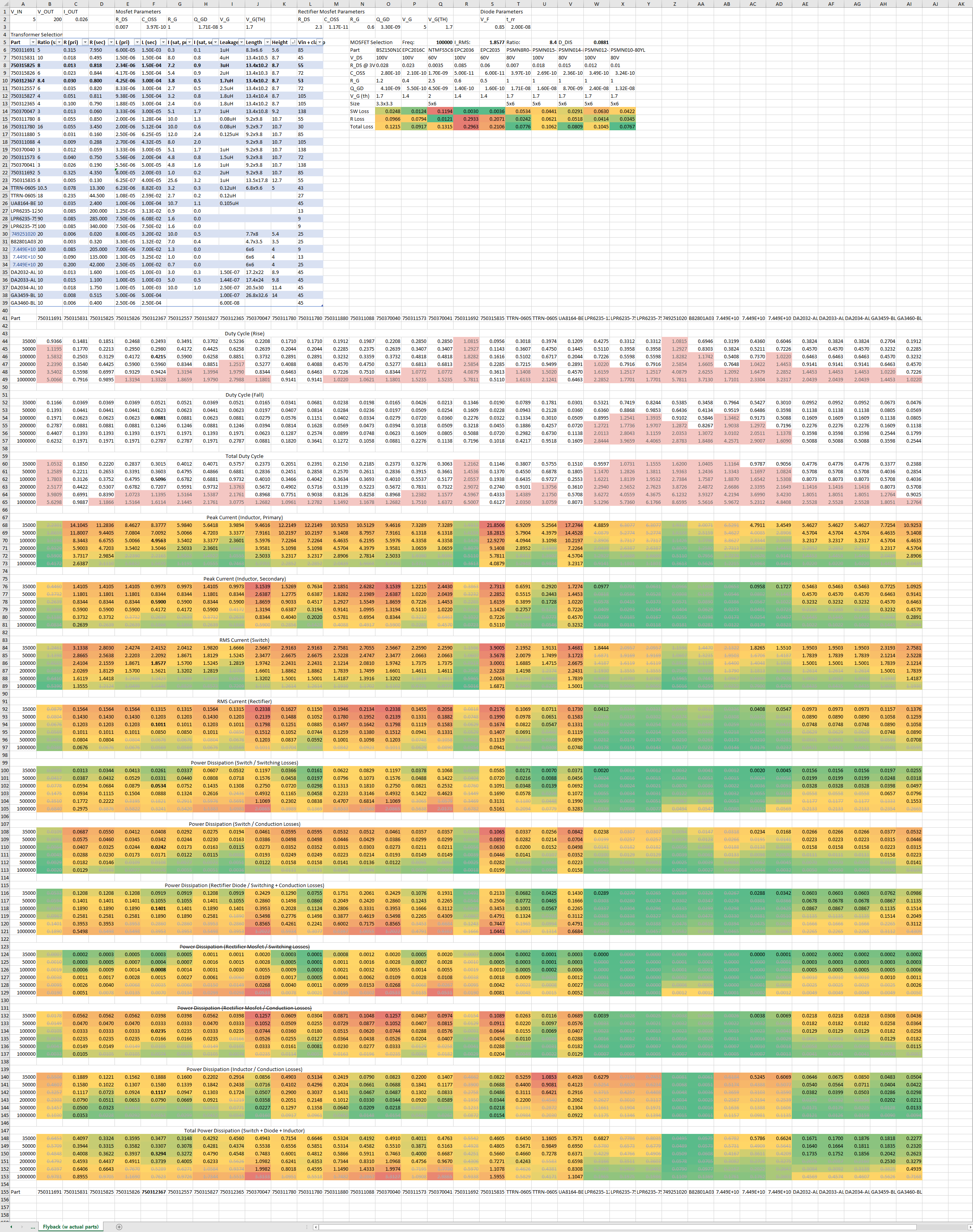
To get a better understanding of the various parameters involved in component selection, I created a few spreadsheets to solve for various parameters (Ddcm, Ddis, Ipk, Irms, PdS, PdL, and PdD) of the circuit across a range of inductance and switching frequencies for both boost and flyback topologies. From these sheets, it’s easy to see that a flyback circuit has lower overall power loss in the inductor(s), switch, and rectifier.
Transformer Selection
For the transformer, I filtered the options available on Digikey for surface mounted transformers between 8mm and 11mm in height. Anything smaller had either too high of an inductance value, low winding ratio, or a low saturation current. I took the options that were available and plugged them into another page in the spreadsheet to compute the duty cycles and estimated power loss. Note that the choice of MOSFET and rectifier were kept the same across all options, even though the MOSFET will likely change depending on the winding ratio of the transformer.
From the results, I looked at a few different combinations of input voltage and output current to get an idea of the power consumption across the range of available transformers. With the minimum input voltage of 3.7V and an output current ranging from 1mA to 25mA, the Wurth 750315825 or 750312367 seems to provide optimal performance when operating at 100kHz. Note that these transformers were originally designed for buck converters, so the windings and their corresponding ratings need to be swapped. Of the two transformers, the 750315825 would have been a better choice due for its lower inductance (which allows for higher output currents), but that part doesn’t seem to exist outside of Wurth’s catalog.
The saturation current rating of the transformer was anothe point of concern given the high peak current through the primary winding of the transformer. To verify that the performance of the transformers, LTSpice simulation was done using the models provided by the manufacturer to verify that the true saturation point (where the current starts to sharply rise) is much higher than the rated saturation current.
TIND = Wurth 750312367
Rated inductance (primary): 4.25µH
Winding ratio: 1:8.4
Resistance (primary): 30mΩ
Resistance (secondary): 800mΩ
Saturation current (primary): 3.8A
Leakage inductance: 1.7µH
Footprint (L×W×H): 13.4mm × 10.2mm × 8.7mm
It may be tempting to use current sense transformers or coupled inductors to take advantage of the high winding ratios that range from 1:20 to 1:100 or more, but the high inductance on the primary winding will limit the maximum output current to only a few milliamps at most before the exceeding 100% duty cycle.
MOSFET Selection
Once the transformer has been picked out, the next step is to choose the switching MOSFET. The expected voltage across the MOSFET is Vin + Vclamp where Vclamp is double the reflected voltage of 24V. This sets a minimum requirement of VDS = 60V. The other important parameters are the on-resistance RDS, output capacitance Coss, and the overall footprint size. Note that the datasheet must be thoroughly examined if the gate drive voltage is close to the threshold voltage as the drain-source resistance will increase exponentially when the gate voltage is low.
The 3.7V input requirement makes it difficult to reduce switching losses at the minimum input voltage. Most MOSFETs, even those with logic level gate thresholds, will exhibit extremely high drain-source resistance at 3.7V. For example, the On-Semi FDMC86160 has a drain resistance of 16mΩ and a gate threshold of only 2.9V, but if you look at the RDS(on) to VGS chart in the datasheet, the drain resistance spikes to an unknown value that could potentially be in the tens or hundreds of ohms at low gate voltages! With an input voltage of 3.7V and an output of 25mA, the MOSFET will see a RMS current of 2.1A which will result in extremely high losses!
Another interesting observation when choosing MOSFETs is that you have to either prioritize the on-resistance or the output capacitance, but not both at the same time. MOSFETs with an extremely low on-resistance of <50mΩ typically have a much larger output capacitance of >300pF. These are a better choice for high output current applications where the conduction losses dominate. MOSFETs with a low capacitance of <300pF on the other hand typically have a larger on-resistance of >200mΩ. These are better for low output current applications where switching losses tends to dominate. This makes sense as a wider switching channel results in lower resistance, but adds more material and therefore more capacitance to the device.
Given that this is a one-off project with efficiency being heavily prioritized, I found a novel MOSFET available on Digikey: the EPC2016C. What makes this part unique is that it is not a traditional Silicon MOSFET, but a Gallium Nitride one that is a only available in passivated die form to keep the on-resistance and gate capacitance to an absolute minimum. The manufacture also provides LTspice models, detailed guides to using eGaN FETs, as well as assembly and layout guidelines for their parts.
QSW = EPC2016C
Max drain to source voltage: 100V
Drain to source resistance: 16mΩ @ 3.7V
Minimum gate voltage: 2.85V
Output capacitance: 210pF
Continuous current: 18A
Footprint: 3mm2
An alternative and potentially better MOSFET that is capable of operating at lower gate voltages and with higher thermal dissipation capabilties is the PSMN014-80YL. For higher output currents, PSMN8R0-80YL has half the on-resistance (8mΩ @ 3.0V!) in exchange for higher output capacitance.
QSW = PSMN014-80YL
Max drain to source voltage: 80V
Drain to source resistance: 15mΩ @ 3.0V
Minimum gate voltage: 2.5V
Output capacitance: 236pF
Continuous current: 62A
Footprint: 30mm2
Rectifier Diode Selection
With the transformer known, the rectifier diode can be chosen. The peak reverse voltage across the diode includes the reflected voltage from the secondary: N{s:p} × Vin + Vout, resulting in a minimum reverse voltage of 300V.
DRECT = UF1GLWHRVG
Max reverse voltage: 400V
Forward voltage: 0.85V @ 200mA
Reverse recovery time: 20ns
Footprint: 8mm2
Input/Output Capacitor Selection
Choosing the input and output capacitors were mainly driven by what was available than a desire for a specific ripple voltage. Ceramic capacitors were chosen for each end: one for bulk capacitance and one for high frequency transients. Capacitors with a voltage rating higher than the required voltage was selected to account for the capacitance drop due to DC bias. This mostly impacted the output capacitors as the 2.2μF capacitor is effectively a 1.43μF capacitor at 200V while the 100nF capacitor turns into a 60nF capacitor at 200V.
Input Capacitors:
CIN (bulk input) =445-14933-1-ND (10µF ± 20%, 50V, X7R, 1210)
CIN (HF bypass) = 445-7856-1-ND (100nF ± 10%, 50V, X7R, 0805)
Output Capacitors:
COUT (bulk input) = 445-7781-1-ND (2.2µF ± 10%, 450V, X6S, 2220)
COUT (HF bypass) = 445-7922-1-ND (100nF ± 10%, 630V, X7R, 1812)
Clamp Component Selection
A DZ clamp is used to protect the MOSFET from the leakage transformer’s leakage inductance. The diode needs to have a reverse voltage rating greater than Vin + Vclamp = 60V as well as being able to handle the peak current of 2.1A. The Zener diode’s reverse breakdown voltage must be below 88V with some extra margin to ensure that the voltage rating of the MOSFET is not exceeded. The Zener diode must also be able to handle a peak load of 625mW. Diode selection was limited by the selection of available footprints, so I just went with the smallest footprint.
DSN = V2PM10HM3/H (100V, 2A, Schottky)
DZSN = BZD27C75P-E3-08 (75V, 800mW)
Components for the clamp circuit was selected to serve as a backup in the event that the the peak voltage did exceed the expected maximum of 90V with the 750312367 as the transformer and the EPC2016C as the switch. If the measured voltage spike remains under the 100V rated limit at maximum output current, the clamp circuit will be omitted from the final design. A snubber circuit across the MOSFET and output rectifier diode was omitted to minimize component count and board size as reducing EMI is not a high priority for this project.
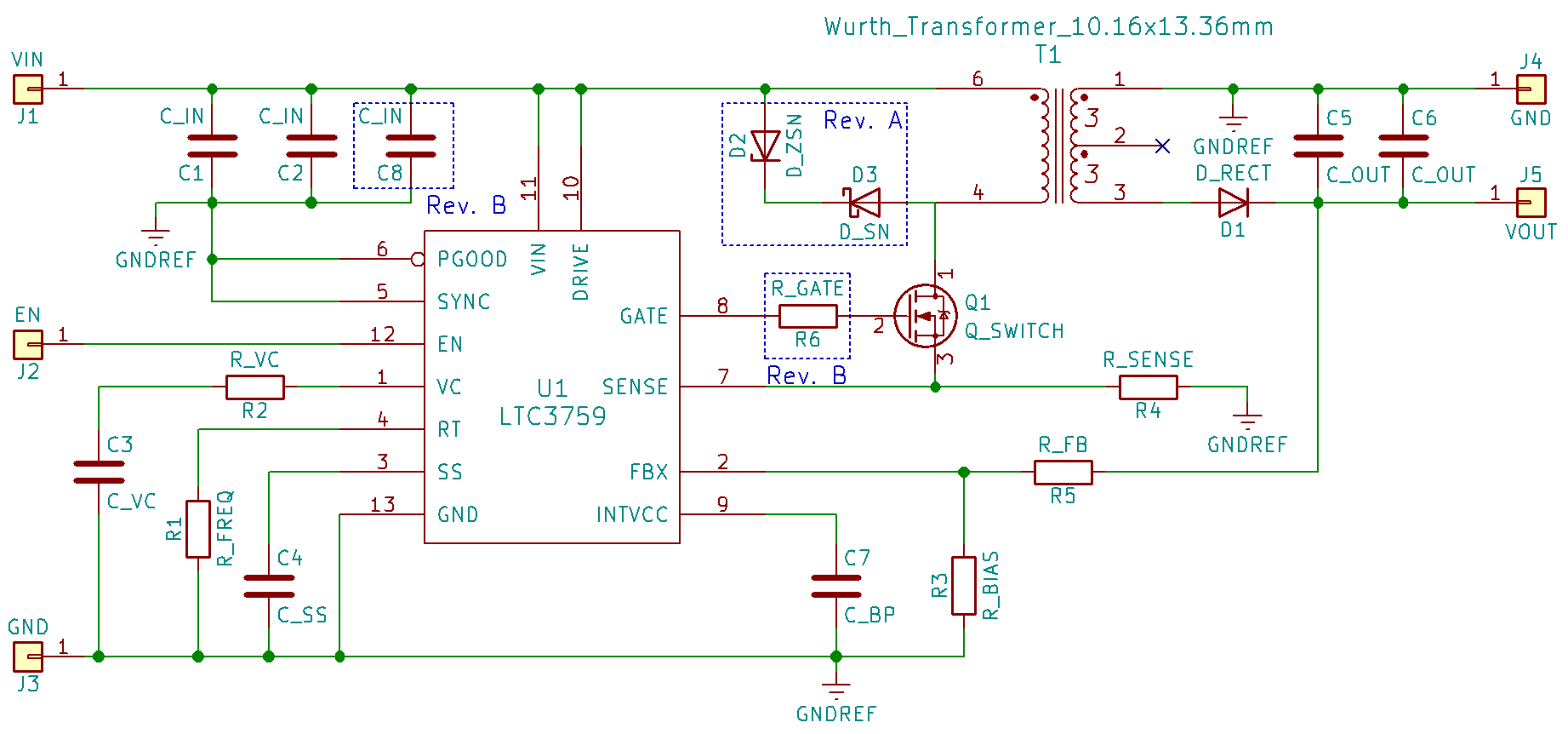
Boost Controller Selection
For this project, I decided to go with the LT3759 for the boost controller. This chip was chosen in particular for its wide operating voltage range from 1.6V to 42V with a regulated gate voltage of either 3.75V (from VIN) or 4.75 (from VDRIVE). A secondary input for the internal voltage regulator from the boost converter’s output allows for a higher gate drive voltage to reduce the switch MOSFET’s on-resistance.
With the EPC2016C, a gate voltage under 2.85V causes a dramatic rise in the drain to source resistance. This is acceptable as lithium-ion batteries operate from 3.0V to ~4.0V and the internal regulator of the LT3786 has a 0.15V drop between Vin and INTVCC when Vin is under 3.9V.
The auxiliary components for the LT3759 can be selected based off of formulas given in the datasheet:
RSENSE = 10mΩ (peak 5A on primary)
RFREQ = 86.6kΩ (for 100kHz)
CSS = 150nF (18ms soft start)
RVC = 300kΩ (from simulation)
CVC = 560pF (from simulation)
RFB = 1.6MΩ (120nA FBX pin input current)
RBIAS = 13kΩ (1.6V at FBX pin)
CBP = 4.7µF (from datasheet)
For lower output currents, the TPS40210 is an interesting alternative with its lower rated operating frequency of 35kHz. For a design optimized for overall footprint, the LT8304 has a built-in 2A 150V switch for a larger reduction in component count, with the trade-off being somewhat lower efficiency.
LTspice Simulation
Prior to finalizing the components and laying out the PCB, some simulation was done in LTspice to verify that the circuit operated as expected in a somewhat ideal scenario. Models for the transformer and the boost controller were provided by the manufacturer, and similar components were chosen from the LTspice component library for the MOSFET switch and the rectifier diode. Some important points that were observed:
- The transformer (750312367) fully saturates at a peak of 5A. This limits the output current to a maximum of ~20mA regardless of the input voltage.
- Make sure the transformer is using the saturation model rather than the default linear model.
- A fast recovery diode for the output rectifier is absolutely necessary. The reverse recovery time is a major factor in how much energy is transferred to the output capacitors.
- No significant voltage spike or ringing was observed on the switching node.


Design Specifications
| Parameter | Symbol | Test Conditions | Min | Typ | Max | Unit |
| Input Voltage | Vin | Ambient = 25°C | 3.0 | 3.7 | 12 | V |
| Input Current | Iin | Vin = 3V, Iout < 25mA, η = 90% | 1.17 | 2.33 | A | |
| Vin = 12V, Iout < 25mA, η = 90% | 0.65 | 1.29 | ||||
| Output Voltage | Vout | RFB = 1.6MΩ, RBIAS = 13kΩ | 195 | 200 | 205 | V |
| Output Current | Iout | | 10 | 20 | mA | |
| Output Overcurrent | Iout(max) | RSENSE = 10mΩ | 20 | mA | ||
| Switching Frequency | FS | RFREQ = 86.6kΩ | 100 | kHz | ||
| Typical Efficiency | ηpk | Vin = 3V, Iout = 10mA | > 80 | % | ||
| Vin = 12V, Iout = 10mA | > 85 | |||||
| Full Load Efficiency | η | Vin = 3V, Iout = 20mA | > 90 | % | ||
| Vin = 12V, Iout = 20mA | > 90 | |||||
| Operating Temperature Range | Top | -20 | 25 | 125 | °C | |
Schematic
Bill of Material
| Reference | Description | Footprint | Part Number |
| C1 | CIN – Ceramic, 10µF ± 20%, 50V, X7R | 1210 | 445-14933-1-ND |
| C2 | CIN – Ceramic, 100nF ± 10%, 50V, X7R | 0805 | 445-7856-1-ND |
| C3 | CVC – Ceramic, 560pF ± 10%, 50V, X7R | 0603 | 445-5649-1-ND |
| C4 | CSS – Ceramic, 150nF ± 10%, 50V, X7R | 0603 | 445-6925-1-ND |
| C5 | CBP – Ceramic, 4.7µF ± 10%, 35V, X5R | 0603 | 445-9064-1-ND |
| C6 | COUT – Ceramic, 2.2µF ± 10%, 450V, X6S | 2220 | 445-7781-1-ND |
| C7 | COUT – Ceramic, 100nF ± 10%, 630V, X7R | 1812 | 445-7922-1-ND |
| C8 2,3 | CIN – Ceramic, 10µF ± 20%, 50V, X7R | 1210 | 445-14933-1-ND |
| D1 | DRECT – Diode, 400V | SOD-123W | UF1GLWHRVGCT-ND |
| D2 1 | DZSN – Zener, 75V, 0.8W | DO-219AB | BZD27C75P-E3-08GICT-ND |
| D3 1 | DSN – Schottky, 100V, 2A | MicroSMP | V1PM10-M3/HGICT-ND |
| Q1 2 | QSW – MOSFET, N-channel, EPC2016 | 2.1mm × 1.4mm | 917-1080-1-ND |
| Q1 3 | QSW – MOSFET, N-channel, PSMN014-80YL | 5mm × 6mm | 1727-2590-1-ND |
| R1 | RFREQ – Resistor, 86.6kΩ, 1/10W, 1% | 0603 | P86.6KDBCT-ND |
| R2 | RVC – Resistor, 300kΩ, 1/10W, 1% | 0603 | P300KHCT-ND |
| R3 | RBIAS – Resistor, 13kΩ, 1/10W, 0.1% | 0603 | P13.0KHCT-ND |
| R4 | RSENSE – Resistor, 10mΩ, 1/2W, 1% | 0805 | P.01AQCT-ND |
| R5 | RFB – Resistor, 1.6MΩ, 1/10W, 1%, 350V | 0603 | RHM1.6MAYCT-ND |
| R6 2 | RGATE – Resistor, 20Ω, 1/10W, 1% | 0603 | P20.0HCT-ND |
| T1 | TIND – Transformer, 4.25µH, 1:8.4 | 13.4mm × 10.2mm | 1297-1017-1-ND |
| U1 | IC – Boost Controller, LT3759 | MSOP-12 | LT3759EMSE#TRPBFCT-ND |
1 Rev. A layout only
2 Rev. B layout only
3 Rev. C layout only
Rev. A PCB Layout and Analysis
The high speed operation of a boost converter PCB requires careful attention to board layout and component placement. To prevent EM radiation and high frequency coupling into signal lines, proper layout of all components on the PCB is necessary. This is especially true for components around paths that contain fast changes in current (high di/dt) to reduce inductive ringing. In a boost topology, this loop contains the output capacitor, the sense resistor, the MOSFET switch, and the rectifier diode. In a flyback topology, the primary loop contains the input capacitor, the primary winding of the transformer, the MOSFET switch, and the sense resistor. The secondary loop contains the output capacitor, the secondary winding, and the rectifier diode.
As usual, there are a number of excellent resources on this topic. The set of guidelines that I followed:
- Use a Kelvin connection between the sense RSENSE and the SENSE pin
- Keep high current paths away from the FBX pin
- Place the divider resistors near the FBX pin to keep the high impedance FBX node small
- Keep RVC and CVC near the VC pin for similar reasons
- Bypass capacitors should be kept close to the IC
- No ground plane under the inductor/transformer
- Ground RSENSE with multiple vias to reduce parasitic resistance and inductance
- Keep the trace from the GATE pin to the MOSFET short
Following these guidelines, I was able to lay out the components on a 29mm × 16mm PCB.

")


- Having a correct solder mask for the EPC2016C is absolutely critical due to the pad sizes.
- Under-sizing the solder mask is recommended as some solder paste will get underneath the stencil.
- The transformer should be manually soldered to avoid melting the tape.
Once the board was assembled, I scoped a number of nodes on the PCB to find any potential issues with the design and layout. For the most part, my power supply look nominal. The output voltage was steady at 198V across the 3V to 12V input range. Most of the waveforms from the various nodes in the circuit looked correct as well, with the only exception being some unexpected ringing at the source node (voltage across the sense resistor). Originally I thought that I may have damaged the MOSFET from excessive heat when I had to fix a solder joint, but the issue persisted even after replacing the MOSFET. Some observations:
- Ringing at the drain node peaked at ~50V with a peak of 5A in the primary winding.
- The controller limited the current in the primary loop to 5A (50mA) as designed.
- Gate drive was operating at the expected voltage across the input range.
- MASSIVE ringing at the source node when the MOSFET switched on and off.
- Ringing increased with higher input voltages.
- Same measurement for the NCH8200HV was done as well for comparison.
- Building a variable resistive load capable of sinking 5W out of discrete resistors is rather difficult to do.


Rev. B PCB Layout and Analysis
For the second revision of the board, I wanted to address the following concerns:
- Add a gate resistor between the gate driver pin and the gate of the MOSFET.
- Increase the number of vias connecting components to the ground plane.
- Route input loop on a single ground pour (no vias in the critical path).
- Route sense resistor ground and IC ground on the same ground pour to reduce ground bounce.
- Remove the clamping diodes as they are unnecessary for the peak current of this transformer.
- Add an additional input capacitor to further reduce input ripple.
- Use OSHpark’s option for 0.8mm PCBs with heavier 2oz copper.
With these changes, I was able to lay out the components on a slightly smaller 22mm × 17mm PCB.
")
")
")
- Overall, the second revision had much lower noise and fewer anomalies in the output waveforms.
- The ringing at the drain of the MOSFET was still there, but peaked at a significantly lower voltage.
- There was a significant efficiency improvement at low input voltages (less than 5V).
- Overall effiiency was otherwise identical between the first and second revisions. This was expecially odd since there was a ~10% efficiency gain at 3V between the two revisions.
- Output current at 3V was actually limited by the thermal dissipation ability of the MOSFET. It turns out, the EPC2016C can only handle ~2A of continuous current before it shorted and started to smoke.
- The efficiency at 3V decreased with output current due to the thermal issue above; higher temperatures results in higher on-resistance of the MOSFET, which eventually overheats due to the positive feedback loop.


Rev. C PCB Layout and Analysis
While the second version utilizing the EPC2016 met the efficiency goals, it still had a major issue to iron out: the MOSFET had a tendency to overheat and short out when operated continuously at the maximum output current supported by the transformer (~20mA). This is due to a positive feedback loop between the MOSFET’s on-resistance and the operating temperature: higher temperatures increase the on-resistance, which given a constant current will cause further higher power drawn by the MOSFET. Once this happens, damage to the MOSFET is very likely as the thermal dissipation capability of the EPC2016 is pretty terrible due to it’s size. As such, for the third revision, I decided to replace the EPC2016 with the PSMN014-80YL. This MOSFET has similar characteristics, but comes in a much larger LFPAK56 package.


- There was almost no ringing at the source node of the MOSFET, even with no gate resistor.
- The input voltage could go as low as 2.2V before the drain-source resistance became too high.
- At higher input voltages, the transformer saturates before the MOSFET overheats.


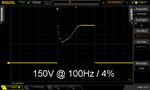
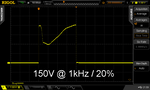
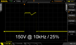
Efficiency Analysis
In addition to looking at the waveforms in isolation, I also charted some higher level comparisons between my power supply revisions and the NCH8200HV. Data source for the comparison charts can be found in this document. Input and output measurements were made using a combination of my bench power supply and multimeters. A separate voltage rail from the power supply was used to feed a range of supply voltages to the PCA968 ICs on the driver PCB with a few of the Nixie tubes turned on, thereby controlling the output current from the power supply. While this setup worked, it wasn’t ideal as I had to manually change the supply voltage for each measurement point.
Generally speaking, all revisions of my layout had similar results with higher input voltages, with near-identical output efficiency when operating between 5V and 12V. At lower input voltages however, the third revision had significantly higher overall efficiency and was also capable of sustaining the maximum output current as limited by the inductance saturation point of the transformer.
The NCH8200HV did have higher efficiency at low output currents (<4mA), but my design had slightly higher efficiency otherwise. One thing to note is that the NCH8200HV has a default lower output voltage of ~170V compared to the ~200V of my design. Dropping my output voltage to 170V adds ~1% efficiency across the board.


The second difference is in the MOSFET used by the NCH8200HV. With a transformer with a higher winding ratio, a MOSFET with a lower VDS rating can be chosen. Lower the VDS rating has two major benefits: the RDS on-resistance can be reduced from the >15mΩ of the EPC2016C down to <10mΩ with the overall capacitance also often being lower as well. The combination of a lower winding ratio and higher on-resistance MOSFET in my design is the likely explanation for the lower efficiency at low input voltages.
Concluding Remarks
In the end, I managed to achieve my goal of a 90% efficient power supply with a wide 3V to 12V input voltage and a fixed 200V output. Is there still room for improvement? Certainly. Was it worth the time and effort to design a custom power supply for this project? For me, absolutely. My intention from the start was to learn and get experience with designing a power supply completely from scratch. For most others though, I suspect that simply using the NCH8200HV is a better choice. Not only do you get nearly the same performance, but the height of the NCH8200HV is a bit smaller as well due to the transformer having a significantly lower profile. For those that want to design their own power supply, I hope that the resources provided here prove to be useful in your quest to do so.
Controller Board
After all the power related concerns for driving Nixie tubes have been resolved, the next step is to design the controller PCB that contains the microprocessor along with additional supporting components for the intended functionality. These include the real-time clock, audio driver and amplifier, battery holder and charger, backlight LED driver, GPS, wireless communication ICs, and more.
Microcontroller
There were two main drivers behind the choice of microcontroller for this project. The first is that I wanted to use a chip/architecture that I have not used before in any of my previous projects. The second is to continue with the open-source nature of this project and build upon a platform that has an open and easily available toolchain. For obvious reasons, I also wanted to use something that is at least somewhat popular/common in the industry to gain some experience working with the architecture at a very low level.
After going through a bunch of options, I ended up with the STM32L432KC, an ARM Cortex-M4 based microcontroller that has an impressive list of features:
- High performance, with operation up to 80MHz
- Internal RTC with support for calendar, alarms, and calibration
- Supports external battery for maintaining RTC time
- Three capacitive sensing channels
- 256KB Flash, 64KB SRAM
- One 12-bit ADC, two 12-bit DACs with optional output buffer
- One configurable internal op-amp
- Built-in support for USB2.0
- SAI (audio) bus support in additional to the usual I2C/USART/SPI/CAN buses
- True random number generator
- Programmable via both SWD and JTAG
This microcontroller also comes in an affordable ($11) development platform, the NUCLEO-L432KC. This platform also happens to be have support for the Mbed OS, an open-source embedded operating system with an online-based compiler. The board itself contains a ST-LINK/V2-1 for programming the onboard microcontroller , making it easier to start prototyping without having to buy an external programmer.
Reference documents for the STM32L432KC:
- Datasheet
- Reference manual
- Cortex-M4 programming manual
- Cortex-M4 generic user guide
- Nucleo-32 user manual
ARM CMSIS/HAL
To reduce development effort, time, and cost, ARM provides a common abstraction layer for generic hardware on ARM-based microcontroller:
The Cortex Microcontroller Software Interface Standard (CMSIS) is a vendor-independent hardware abstraction layer for the Cortex®-M processor series and defines generic tool interfaces. The CMSIS enables consistent device support and simple software interfaces to the processor and the peripherals, simplifying software re-use, reducing the learning curve for microcontroller developers, and reducing the time to market for new devices.
ST also provides an additional abstraction layer for their STM32 microcontrollers that has support for additional hardware peripherals:
The STM32Cube Hardware Abstraction Layer (HAL) is an STM32 embedded software stack that ensures a maximized portability across STM32 portfolio, while the Low Level (LL) APIs make up a fast, light-weight, expert-oriented layer which is closer to the hardware than the HAL. HAL and LL APIs can be used simultaneously. Both the HAL and LL APIs are production-ready and have been developed in compliance with MISRA-C guidelines and ISO/TS 16949. On top of that, ST specific validation processes add a deeper-level qualification.
CMSIS uses the following essential coding rules and conventions:
- Compliant with ANSI C (C99) and C++ (C++03).
- Uses ANSI C standard data types defined in <stdint.h>.
- Variables and parameters have a complete data type.
- Expressions for #define constants are enclosed in parenthesis.
- Conforms to MISRA 2012 (but does not claim MISRA compliance).
All code examples and resources provided by ARM have been tested and verified with the following compilers:
- Arm Compiler
- GNU Tools for Arm Embedded
- IAR ANSI C/C++ Compiler for Arm
The GNU Arm Embedded Toolchain is also available as a standalone package, which combined with CMSIS allows the source code for this project to be compiled without having to install anything on the base machine. For Ubuntu 16.04 and onward, the latest toolchain also be installed from the GNU ARM Embedded Maintainer’s PPA:
|
1 2 3 |
sudo add-apt-repository ppa:team-gcc-arm-embedded/ppa sudo apt-get update sudo apt-get install gcc-arm-embedded |
Packages can also be directly installed on newer releases:
|
1 2 3 |
sudo apt-get install gcc-arm-none-eabi sudo apt-get install binutils-arm-none-eabi sudo apt-get install gdb-arm-none-eabi |
For the STM32L432KC, both CMSIS and HAL are bundled into one package: the STM32CubeL4. Many additional resources are also provided in this package, such as templates and resources files for the NUCLEO-L432KC and various high level peripheral libraries.
Debugging via SWD
If you’re only looking to build and flash binaries to the microcontroller, the instructions above should be sufficient with my code as reference. If you’re planning on doing any sort of development work however, you’ll want a way to debug running code. There are a few different ways that one can go about debugging STM32 microcontrollers:
- Serial Wire Viewer (ST-Link) via Instrumentation Trace Macro cell (ITM) – Serial Wire Output (SWO) interface
- Extremely fast, but limited to one way communication (microcontroller to host)
- Not supported on some NUCLEO development boards (Nucleo-32 series)
- GDB via semihosting (CMSIS-DAP) – Serial Wire Debug (SWD) interface
- Extrememly slow. Eclipse plugin available for in-IDE debugging via printf
- GDB via J-Link – JTAG interface
- Not supported on some NUCLEO development boards (Nucleo-32 series)
- Putty via Virtual Com Port (VCP) – UART interface
- Requires an onboard ST-LINK programmer
- Putty via Serial – UART interface
- Requires an external Serial to USB adapter
For native debugging over SWD/GDB on the NUCLEO-L432KC using the onboard ST-LINK, you’ll need to first download and/or install an intermediate GDB server such as OpenOCD (0.10.0+). On Windows, you can download and run from the standalone pre-built binaries. On Ubuntu/WSL 18.04 and newer, you can directly install OpenOCD via apt-get. An alternative option for the GDB server is pyOCD.
First start a OpenOCD session on the host machine that the NUCLEO-L432KC is connected to:
|
1 |
openocd -f board/stm32l4discovery.cfg |
Then start GDB pointing to the binary to run on the microcontroller:
|
1 |
arm-none-eabi-gdb main.axf |
Once GDB has started, attach to OpenOCD, load the binary, and begin execution:
|
1 2 3 4 5 6 |
target remote localhost:3333 monitor arm semihosting enable monitor reset halt load monitor reset init continue |
If you are debugging via printf, the debug messages will start appearing in the OpenOCD window.
ST-LINK/V2
The ST-LINK/V2 on the NUCLEO-L432KC is only capable of connecting to the onboard microcontroller, but a basic standalone ST-LINK programmer can be easily obtained via Ebay for $5. These cheap Chinese knockoffs are a hardware clone of the official ST-Link/V2, which allows for debugging via SWD (for STM32) and SWIM (for STM8). It’s possible to support for SWO debugging to the knockoff ST-LINK/V2 as well with an easy hardware hack.
For more extensive debug capabilities using SWO or JTAG, you’ll need to either use the a ST-LINK/V2 programmer from a more-capable NUCLEO board (ex. NUCLEO-F446RE) or a high performance external debugger (ex. Segger J-Link) which has support for far more than just STM32 microcontrollers. As far as value goes, the NUCLEO option is the better choice due the lower cost (<$14) vs the high cost of the Segger J-Link ($60 for the J-Link EDU). The NUCLEO boards with JTAG connectivity also can be upgraded free-of-charge to J-Link as well for more features and significantly improved performance.
- ST-LINK utility (Windows)
- ST-LINK firmware update
- ST-LINK USB driver (Windows)
ROM Bootloader
To avoid the requirement of always having to use an ST-LINK for programming the board, newer STM32 microcontrollers comes with an integrated bootloader stored in the internal boot (system) memory. Depending on the BOOT0 pin value and/or the nSWBOOT0/BOOT1 register flags, the device can be configured to boot from the integrated ROM bootloader to load a new firmware over CAN, I2C, SPI, USART, or USB.
One of the more useful features that this enables is the ability to reprogram the flash memory by putting the device into the USB device firmware update (DFU) mode. Once in the device is in this mode, the microcontroller will be able to enumerate over USB as a DFU device and subsequently download and flash a new firmware with the help of an external utility (DfuSe or dfu-util).
ST Micro’s microcontrollers uses its own DFU extension (v1.1a), which is not backwards compatible with the DFU standard (v1.1). For these microcontrollers, the DfuSe upload utility (DfuSeDemo) can be used to upload a *.dfu files that are generated using the Dfu file manager utility. These files contain the target binary along the address to write the binary to in memory, and are created from S19, hex, or bin source binary files. The command line utility dfu-util contains DfuSe support as well and can upload the source binary directly, bypassing the need to create a *.dfu file. If you really need to generate a *.dfu file via the command line, there is a python script available as well.
To upload a DFU file using dfu-util, run:
|
1 |
dfu-util -a 0 -D your-firmware-file.dfu |
To download a raw binary to the flash address space (0x08000000):
|
1 |
dfu-util -a 0 --dfuse-address 0x08000000 -D target_binary.bin |
One thing to note is that both dfu-util and DfuSeDemo can be quite unreliable for uploading files, and often requires a few tries before it is able to successfully sync with the internal DFU state machine. This may be due to a bug in some versions of the DFU bootloader for this family of microcontrollers. I did confirm however that a local build of DfuSeDemo with the source code modification as described in this thread fixed the the reliability issue.
- DfuSe USB device firmware upgrade utility
- DfuSe USB device firmware upgrade user manual
- STM32 System memory boot modes
- STM32 Bootloader CAN protocol
- STM32 Bootloader I2C protocol
- STM32 Bootloader SPI protocol
- STM32 Bootloader USART protocol
- STM32 Bootloader USB DFU protocol
Custom Controller PCB
To ensure that all the basic functionality is correctly implemented, the first revision of the PCB will be pretty sparse:
- ARM R4 microcontroller
- USB type-C receptacle and ESD components
- External temperature compensated RTC
- Button cell battery for maintaining RTC time
- High voltage power supply and protection circuitry
- Buck/boost power supply for ICs
- DAC voltage buffer for LED drivers
USB Type-C
To both program and power the device over a single cable, I decided to use the built-in USB peripheral of the STM32L4 with a USB Type-C connector for future-proofing. USB Type-C natively supports up to 3A @ 5V, but for more power hungry applications, the full Power Delivery (PD) protocol can be implemented to obtain up to 5A @ 20V over the same cable. For backwards compatibility with USB 2.0 power adapters, the STM32L4 also has built in detection support for the USB 2.0 Battery Charging (BC) 1.2 specification.
Implementing the full power delivery (PD 3.0) specification is a non-trivial task, but there are standalone USB Type-C controllers that could make things easier such as the FUSB302B, STUSB1602, and STUSB4500.
| Specification | Maximum Voltage | Maximum Current | Maximum Power |
| USB 2.0 | 5V | 500mA | 2.5W |
| USB 3.0/3.1 | 5V | 900mA | 4.5W |
| USB BC 1.2 | 5V | 1.5A | 7.5W |
| USB Type-C 1.2 | 5V | 3A | 15W |
| USB PD 3.0 | 20V | 5A | 100W |
The TUSB322 port controller was selected to handle the configuration channel (CC) logic required for cable enumeration, current modes, and role detection. The ESD112 chip was chosen for ESD protection on the CC and data lines, while the TPD1E05U06 was chosen for ESD protection for the main Vbus power rail.
- Primer on USB Type-C and Power Delivery (TI)
- Introduction to USB Type-C (Microchip)
- The Basics of USB Battery Charging: A Survival Guide
- Designing In USB Type-C and Using Power Delivery for Rapid Charging
- Preventing ESD Arcing in a Connector
Auxiliary ICs
Due to the way that MOSFETs tends to fail with drain pin shorted to the source pin, I figured that it would be a good idea to have some way to detect over-current conditions via a PTC or eFuse. Since I want to be able to detect this condition in real-time, I opted to go with an eFuse: the TPS259530. Notable features of this IC is that it supports:
- Wide operating voltage from 2.7V to 18V
- Adjustable current limit from 0.5A to 4A
- Adjustable output slew rate control
- Built-in output over-voltage clamp to 5.7V
- Outputs a voltage corresponding to the load current
The current monitor gain (GIMON) can be used to calculate the load current from the IILM pin of the TPS259530. With the maximum possible gain of 300μA/A and a 1kΩ resistor on the IILM pin to set the current limit to 2A, a load current of 2A will result in a pin voltage of 0.3V on the IILM pin. This is important to note as there is an upper limit to the ADC input voltage on the microcontroller. As a large tantalum bulk capacitor is attached to the output of this IC, the inrush current should be limited to a slew rate under 6V/ms to avoid the overcurrent limit of 2A.
To generate the power supply rail for the microcontroller and other ICs incapable of operating off the 5V USB voltage rail, a high efficiency integrated buck/boost converter was used: the TPS630250. While this revision only requires a buck converter to generate the 3.3V rail, in future revisions I may be drawing power from a battery that may drop to a lower voltage. Using this IC ensures that I can reuse as many components of my design between revisions. Notable features of this IC include:
- Automatic seamless transition between operating modes
- Input voltage from 2.3V to 5.5V with an output current of up to 2A (boost) or 4A (buck)
- >90% efficiency @ ~1mA output, up to 97% in ideal operating conditions
- 35μA operating quiescent current with power saving mode (PFM)
- Requires only a single 1μH inductor and input/output capacitors to operate
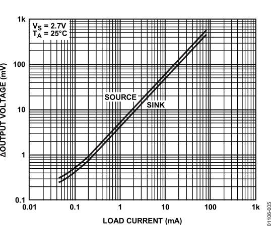
While the STM32L4 has an optional internal voltage buffer at the output of the DACs, some brief testing with the NUCLEO-L432KC revealed that this buffer was insufficient for powering the three PCA9685 PWM drivers. To address this, an external op-amp configured in voltage follower mode is used as a current buffer between the microcontroller’s DAC and the supply voltage for the PWM drivers. The AD8591 chosen has the following features:
- Wide operating voltage range from 2.5V to 6V
- High output current of ±250mA
- Rail-to-rail operation for both input and output
- Low output voltage drop (100mV @ 20mA)
An important parameter to look for when selecting an op-amp operating as a current buffer is the output voltage to supply rail vs load current characteristic. A high load current will result in a voltage drop within the op-amp due to it’s internal resistance, which manifests as a voltage drop between the desired and actual output voltage. For op-amps not capable of high output currents, this difference can be in the hundreds or thousands of millivolts!
The last component is the actual timekeeping IC. While the STM32L432KC has a fully featured internal RTC, it lacked one critical component: an input voltage pin for an external battery. On this particular microcontroller, the VBATT input is connected to VDD, so I would have to either lose RTC time when disconnected from power or implement a system for powering the microcontroller from a button cell battery. Neither are acceptable, so I decided to use an external IC instead. The RTC of choice was the DS3231 which has the following features:
- Has an integrated temperature-compensated crystal oscillator (TXCO)
- Accuracy of ±2ppm in normal operating conditions
- Digital temperature sensor
- Programmable square wave output to feed to the microcontroller
Schematic
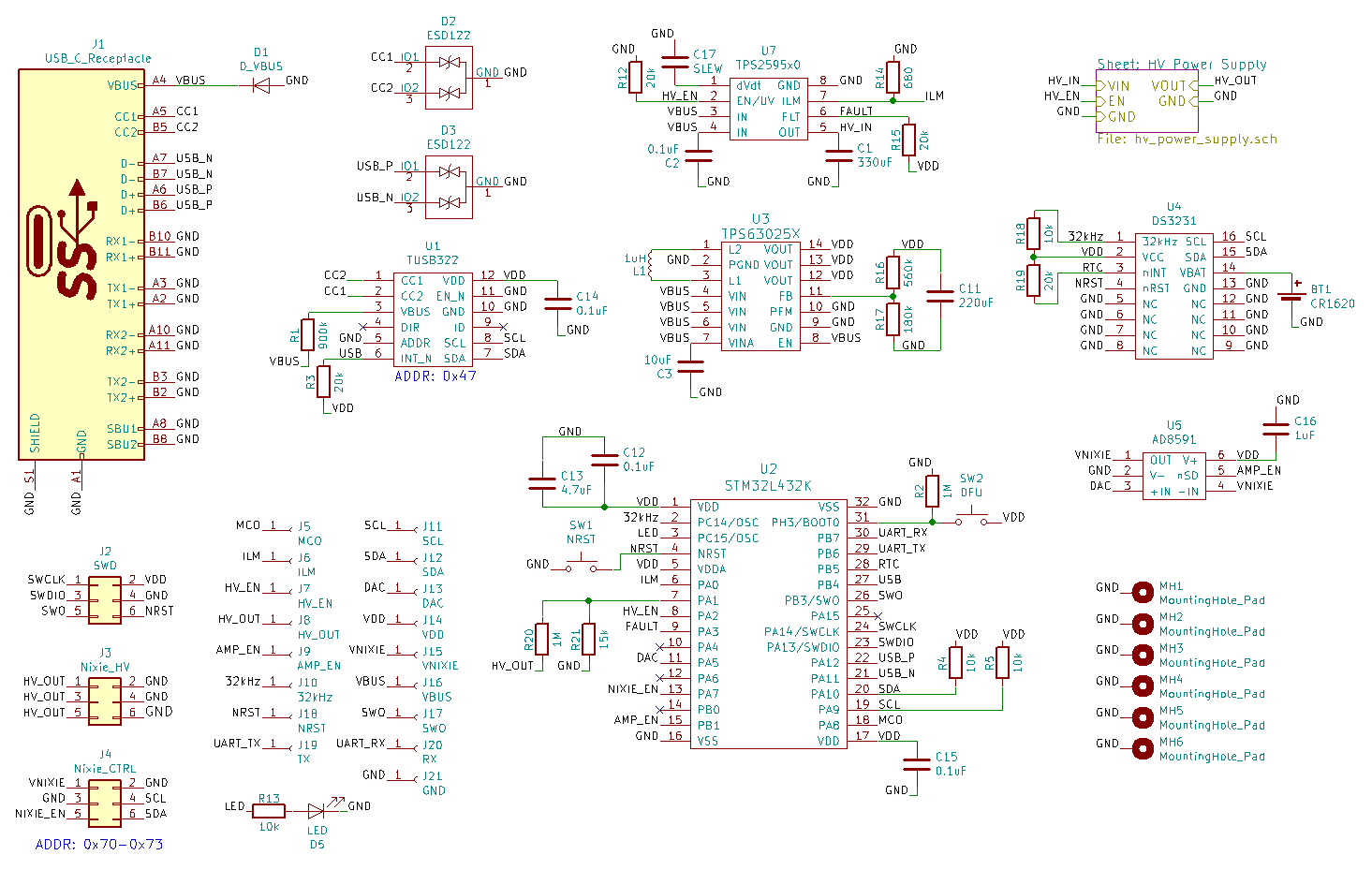
Bill of Material
| Reference | Description | Footprint | Part Number |
| BT1 | Battery Holder – CR1620/1632 | 17.5mm × 18.5mm | BK-869-ND |
| C1 | Tantalum Polymer – VBUS Bulk, 330μF, 6.3V | 7343 | P122483CT-ND |
| C2, C12, C14, C15 | Ceramic – VDD Bypass, 0.1μF, 50V | 0603 | 490-5798-1-ND |
| C3 | Ceramic – VBUS Bypass, 10μF, 16V | 0805 | 1276-3024-1-ND |
| C11 | Ceramic – VDD Bulk, 47μF, 10V | 1210 | 490-5312-1-ND |
| C13 | Ceramic – VDD Bypass, 4.7μF, 16V | 0603 | 1276-1784-1-ND |
| C16 | Ceramic – VDD Bypass, 1μF, 16V | 0603 | 1276-6613-1-ND |
| C17 | Ceramic – eFuse Slew Rate, 10nF, 50V | 0603 | 445-5662-1-ND |
| D1 | Diode – ESD, TPD1E05U06 | X1SON | 296-39341-1-ND |
| D2, D3 | Diode – ESD, ESD122 | DMX0003A | 296-48543-1-ND |
| D5 | LED – Status (Red) | 0603 | 511-1581-1-ND |
| J1 | USB Type-C Port – Female | 9.2mm × 9.1mm | ED1472CT-ND |
| J2 | Tag Connect – TC2030-MCP-NL | 6.0mm × 3.0mm | N/A |
| J3, J4 | Header – Harwin Datamate L-Tek, Female | 5.3mm × 9.0mm | 952-2077-ND |
| J5-J18 | SMD Test Pad | 1.5mm | N/A |
| L1 | Inductor – Buck/Boost, 1μH | 4.1mm × 4.1mm | SRP4020FA-1R0MCT-ND |
| R1 | Resistor – 900kΩ, 1/10W, 1% | 0603 | P910KHCT-ND |
| R2 | Resistor – 1MΩ, 1/10W, 1% | 0603 | P1.00MHCT-ND |
| R3, R12, R15, R19 | Resistor – 20kΩ, 1/10W, 1% | 0603 | P20.0KHCT-ND |
| R4, R5, R13, R18 | Resistor – 10kΩ, 1/10W, 1% | 0603 | P10.0KHCT-ND |
| R14 | Resistor – 680Ω, 1/10W, 1% | 0603 | P680HCT-ND |
| R16 | Resistor – 560kΩ, 1/10W, 1% | 0603 | P560KHCT-ND |
| R17 | Resistor – 180kΩ, 1/10W, 1% | 0603 | P180KHCT-ND |
| R20 | Resistor – 1.6M, 1/10W, 1%, 350V | 0603 | RHM1.6MAYCT-ND |
| R21 | Resistor – 24kΩ, 1/10W, 1% | 0603 | P24.0KHCT-ND |
| SW1, SW2 | Button Switch – SPST-NO | 4.7mm × 3.5mm | P12299SCT-ND |
| U1 | IC – USB Type-C Controller, TUSB322 | 12-XFQFN | 296-43704-1-ND |
| U2 | IC – Microcontroller, STM32L432K | 32-UFQFN | 497-16578-ND |
| U3 | IC – Buck/Boost Controller, TPS630250 | 14-VFQFN | 296-47380-1-ND |
| U4 | IC – TXCO RTC, DS3231 | 16-SOIC | DS3231SN#T&RCT-ND |
| U5 | IC – CMOS Rail-To-Rail Op-Amp, AD8591 | SOT-23-6 | AD8591ARTZ-REEL7CT-ND |
| U7 | IC – Electronic Fuse, TPS259530 | 8-WFDFN | 296-47954-1-ND |
See the HV power supply BoM for components U6, Q1, T1, D4, C4-C10, and R6-R11 (references are different).
Rev. A PCB Layout
Layout of the controller board PCB took a while due to the footprint constraint. The first few steps involved the placement of the position-critical components, including the USB type-C connector, headers, mounting holes, and the through-board transformer. The placement of the transformer in particular was critical, as the the stickout was measured to be just under 7mm (the spacing between the two PCBs). As such, there was really only one valid placement for this transformer: directly between two of the Nixie tube sockets.
After placing the position-ciritcal components, the remaining components for the high voltage power supply was placed and routed to keep the input and output loops as small as possible. A large number of vias were used to connect the traces on the top layer to the transformer on the bottom layer and the input loop is larger than in rev. C of the power supply, so the efficiency is likely to be lower. To keep EMI and other side effects (ie. ground bounce) from affecting the high speed components such as the microcontroller or USB signals, the right side of the PCB was reserved for analog circitry with fast current/voltage transients. This includes the high voltage power supply as well as the buck/boost converter for the 3.3V power rail.
The area in the middle between the two mounting holes was reserved for the USB type-C connector as well as supporting components for USB, such as the ESD diodes and CC logic controller. The physical buttons were placed in this area as well to provide mechanical support for the buttons. The left side of the PCB contains the microcontroller and RTC components, with over 80% of the area being used for just the button cell battery holder and RTC IC. The remaining space was used by the microcontroller and other support components, such as the voltage buffer op-amp and pull-up/down resistors.
The main method of programming the microcontroller is via DFU over USB, but a Tag-Connect port was added as backup to allow programming over SWD as well. The SWD connector was routed to match the same pinout as the ST-LINK/V2-1 connector on the NUCLEO-64 (1. VDD 2. SWCLK 3. GND 4. SWDIO 5. NRST 6. SWO). The USB 2.0 traces were speced using an online impedance calculator and four layer specifications from the manufacturer to a differential impedance of ~100Ω. Per the STM32L432KC’s datasheet, no termination resisters were added.
As this was routed on a four layer PCB, the top and bottom layers were used for signal traces while the inner layers were used as power (IN1) and ground (IN2). This allows for controlled ground impedances for differential signals as the distance between the outer layers to the inner layers is smaller than the distance between the inner layers. Test pads were also added for all the important traces on the board to allow for easier debugging access if needed.


 vs PCBWay (Red)")

")


PCBWay vs OSHPark/OSHStencil
In my rush to order from OSHPark after laying out the PCB, I accidentally submitted two drill files where one of them was slightly out-of-date. This resulted in a few undesirable vias being drilled that shorted through all four layers, effectively making the PCBs useless. Luckly for me, PCBWay had reached out to me earlier this year with an offer to sponsor the PCBs for this project, so I was able to order a correct revison of the board for free1 through them.
To keep things fair between the two manufactures, I selected options to keep the PCBWay order as similar as possible to OSHPark’s four layer service while maintaining the same cost per PCB (~$11 each @ 20mm × 100mm). The following features were kept between the same between the two orders: four layer 1.6mm thick PCB, minimum 5/5mil track width/spacing, minimum 0.25mm drill size, ENIG finish, tented vias, and 1oz outer copper thickness. The PCB layout was identical between the two except for the USB data traces and the footprint for the USB type-C connector. As I now have two PCBs that are effectively the same from two different manufactures, I’ll start off the comparison with some photos:
 vs PCBWay (Red)")
 vs PCBWay (Red)")


OSHPark Pros:
- More cost effective at <10 boards
- Tighter solder mask tolerance
- Higher quality 180Tg FR4 substrate
- Higher quality silkscreen2
PCBWay Pros:
- Faster turnaround (5 days)
- 1.5oz copper for inner layers
- Support for smaller plated slots
- No break-off tabs on edges
One snag that I hit with the order from PCBWay was that there is a minimum pad spacing of 0.25mm for the black solder mask option, so I had to switch to a different color after support reached out to me. Due to the USB type-C connector and CC port controller IC, the mininum pad spacing on my PCB was 0.20mm.
Along with the PCBs, I also ordered a stainless steel stencil from PCBWay as well to compare against the same stencil from OSHStencil. Both manufactures offer 4/5/6/8mil thickness options, but OSHStencil offers a thinner 3mil option as well. The quality was identical between the two manufactures, with the two being close enough that I couldn’t discern between the two even at 20x magnification. As far as cost is concerned, the stencil itself was slightly more expensive from OSHStencil ($15) compared to PCBWay ($10), but the shipping from OSHStencil was signficantly cheaper ($3) compared to PCBWay ($21)3.
1 In exchange for a mention and brief review.
2 Silkscreen quality seems to be higher for 4 layer PCBs in general, but this is very dependent on which fab the boards were sent to. I have seen the same quality silkscreen as PCBWay with two layer boards from OSHPark, but your experiences may differ (please me know!).
3 Shipping included PCBs as well, so is likely to be lower for just the stencil.
Rev. A PCB Analysis
Once the PCB was populated, a few areas for improvements was identified:
- The 47μF tantalum capacitor at the output of the 3.3V buck/boost converter causes the tantalum capacitor to short on startup. Replacing this tantalum capacitor with a ceramic capacitor fixed the issue.
- The polarity of the CR1220 button battery holder was reversed. The metal shell of the holder is designed to contact the positive end of the battery, not the negative. Workaround is to use a CR1130 battery instead and isolate the sides of the battery via a plastic spacer. Bumping up the battery size on the next revision to a CR1620/CR1632 may be a good idea as well.
- The pinout of the Tag Connect port is mirrored, leading to some awkward wiring between it and the ST-LINK.
- The USB Type-C connector, TUSB322, STM32, and eFuse ICs are sensitive to prolonged exposure to high temperatures. Signs that the TUSB322 or STM32 may be damaged include:
- USB DFU is only detected in one orientation
- ATTACHED_STATE register always reports as unattached in one orientation
- CURRENT_MODE_DETECT register value is 0x00, even when connected to a high power source
- The ESD112 and TPD1E05U06 diodes are extremely hard to solder with a hot air pencil due to their size and placement location next to the USB Type-C connector.
- Using a reflow oven is recommended as the USB Type-C connector has hard-to-reach SMD pins under the connector. The pushbuttons and LED should be hand soldered if possible to avoid cosmetic damage.


Rev. B PCB Layout
The second revision of the controller board PCB has a few small improvements:
- Fixed battery holder polarity and swapped footprint for a larger sized battery (CR1620).
- Fixed Tag Connect port pinout.
- Broke out UART pins on the STM32 to allow for time configuration directly from PC.
- Better routing of a few signal traces.


Rev. B PCB Analysis
After assembly, there was very little that I could identify as far as points of improvements for future revisions. The main issue that was found during firmware development was the lack of user accessible inputs, so it would be a good idea to add some DIP switches to allow for configuration of settings such as timezone or DST.


Clock Enclosure
The last component of this project involves the case or enclosure around the bottom half of the Nixie tube clock. While I would normally be fine with leaving the PCBs out in the open, this particular project involves high enough voltages that a nasty shock can occur if care is not taken when handling the clock when powered on.
For the first iteration of the case, I wanted to go all out and make a really nice stainless steel enclosure for the clock. As a result, I spent two full weekends in the Microsoft Garage squaring stock and milling out both halves of the enclosure from some stainless steel stock I had lying around. The dimensions ended up being exactly 25mm (D) × 28mm (H) × 105mm (W) and the resulting weight was perfect at a hefty 260g.
The enclosure itself invoes two parts. The bottom half is a mounting base for the controller PCB and doubles as a stand for showcasing the internals of the clock. The top half encloses both the PCBs along with all components other than the Nixie tubes themselves and isolates all voltage and signal traces from outside interference. This piece is milled out of a single piece of stock to avoid any visual discontinuity or gaps.


")
")
")
")
")
")
")
")


")
")


")


")


Acrylic Enclosure
While the end result of the stainless steel enclosure was nearly perfect, I wanted to make an enclosure that could serve to show off the internals as much as possible. For the second and third copies of this clock, I milled two more enclosures out of a solid block of acrylic, along with a copper base for weight and aesthetics.


Enclosure Stand
One aspect of the enclosure that I missed in my design was that in most usage scenarios, the clock will actually be sitting below the user’s line of sight. While this isn’t necesarily a problem as the top of the nixie tubes are somewhat transparent for visibility in such scenarios, the view isn’t nearly as nice compared to viewing it heads-on. To remedy this, I decided to make an accessory for the enclosure to hold the clock at a 15° angle. This piece was machined out of a piece of aluminum rather than stainless steel as the enclosure itself is heavy enough as it is.


")


Clock Firmware
For the clock firmware, I decided to rapidly prototype the initial firmware using the Mbed library to bring the clock to an acceptable level of operation before I work on writing my own firmware from scratch using the ARM CMSIS/HAL. There were three main software features that I wanted to implement for the initial firmware:
- Independent and easily customizable fading of the digits for each tube
- Reading and updating time from the D3231 RTC IC
- Periodic (randomized) cycling through the digits of each tube to prevent cathode poisoning.
|
1 2 3 4 5 6 7 8 9 10 11 12 13 14 15 16 17 18 19 20 21 22 23 24 25 26 27 28 29 30 31 32 33 34 35 36 37 38 39 40 41 42 43 44 45 46 47 48 49 50 51 52 53 54 55 56 57 58 59 60 61 62 63 64 65 66 67 68 69 70 71 72 73 74 75 76 77 78 79 80 81 82 83 84 85 86 87 88 89 90 91 92 93 94 95 96 97 98 99 100 101 102 103 104 105 106 107 108 109 110 111 112 113 114 115 116 117 118 119 120 121 122 123 124 125 126 127 128 129 130 131 132 133 134 135 136 137 138 139 140 141 142 143 144 145 146 147 148 149 150 151 152 153 154 155 156 157 158 159 160 161 162 163 164 165 166 167 168 169 170 171 172 173 174 175 176 177 178 179 180 181 182 183 184 185 186 187 188 189 190 191 192 193 194 195 196 197 198 199 200 201 202 203 204 205 206 207 208 209 210 211 212 213 214 215 216 217 218 219 220 221 222 223 224 225 226 227 228 229 230 231 232 233 234 235 236 237 238 239 240 241 242 243 244 245 246 247 248 249 250 251 252 253 254 255 256 257 258 259 260 261 262 263 264 265 266 267 268 269 270 271 272 273 274 275 276 277 278 279 280 281 282 283 284 285 286 287 288 289 290 291 292 293 294 295 296 297 298 299 300 301 302 303 304 305 306 307 308 309 310 311 312 313 314 315 316 317 318 319 320 321 322 323 324 325 326 327 328 329 330 331 332 333 334 335 336 337 338 339 340 341 342 343 344 345 346 347 348 349 350 351 352 353 354 355 356 357 358 359 360 361 362 363 364 365 366 367 368 369 370 371 372 373 374 375 376 377 378 379 380 381 382 383 384 385 386 387 388 389 390 391 392 393 394 395 396 397 398 399 |
#include "mbed.h" #include "main.h" #include "SWO.h" #include "pca9685.h" #include "tusb322.h" #include "ds3231.h" #include "ioc.h" #include "animation.h" I2C i2c(PA_10, PA_9); // SWO_Channel swo("swo"); #ifdef REVISION_B Serial serial(PB_6, PB_7); #endif typedef enum { Decrementing = 0, Incrementing = 1, } DigitState; typedef struct { DigitState CurrentState; int Value; int PwmStart; int PwmEnd; bool Updated; } Digit; typedef struct { Digit Digits[NUM_DIGITS]; int LastActiveDigit; int RefreshLastDigit; bool RefreshActive; int FadeDuration; } Tube; Tube Tubes[NUM_TUBES]; // Active per-tube configuration Digit Dot; Timeout DotUpdateTimeout; void DotUpdateCallback(void) { int ticks = DOT_FADE_DURATION_US / REFRESH_RATE_US; int step = ((DOT_MAX - DOT_MIN) + ticks - 1) / ticks; if (Dot.CurrentState == Incrementing && Dot.Value < DOT_MAX) { Dot.Value = (Dot.Value + step >= DOT_MAX) ? DOT_MAX : Dot.Value + step; } else if (Dot.CurrentState == Decrementing && Dot.Value > DOT_MIN) { Dot.Value = (Dot.Value - step <= DOT_MIN) ? DOT_MIN : Dot.Value - step; } Dot.Updated = true; if (Dot.Value != DOT_MAX && Dot.Value != DOT_MIN) { DotUpdateTimeout.attach_us(DotUpdateCallback, REFRESH_RATE_US); } } // Macro the per-tube callback function as each callback needs to be defined as // a unique function (callbacks cannot have arguments and are not reentrant) #define TUBE_CALLBACK(x) \ void Tube##x##UpdateCallback(void) { \ int ticks = Tubes[x].FadeDuration / REFRESH_RATE_US; \ int step = ((DIGIT_MAX - DIGIT_MIN) + ticks - 1) / ticks; \ bool activeTube = false; \ for (int i = 0; i < NUM_DIGITS; i++) { \ Digit *digit = &Tubes[x].Digits[i]; \ if (digit->CurrentState == Incrementing && digit->Value <= DIGIT_MAX) { \ digit->Value = (digit->Value + step >= DIGIT_MAX) ? DIGIT_MAX : digit->Value + step; \ digit->Updated = true; \ } else if (digit->CurrentState == Decrementing && digit->Value >= DIGIT_MIN) { \ digit->Value = (digit->Value - step <= DIGIT_MIN) ? DIGIT_MIN : digit->Value - step; \ digit->Updated = true; \ } \ activeTube |= (digit->Value != DIGIT_MAX && digit->Value != DIGIT_MIN); \ } \ if (activeTube) { \ Tube##x##UpdateTimeout.attach_us(Tube##x##UpdateCallback, REFRESH_RATE_US); \ } \ } Timeout Tube0UpdateTimeout; TUBE_CALLBACK(0) Timeout Tube1UpdateTimeout; TUBE_CALLBACK(1) Timeout Tube2UpdateTimeout; TUBE_CALLBACK(2) Timeout Tube3UpdateTimeout; TUBE_CALLBACK(3) void UpdatePwm(Digit *digit, int *lastPwm, bool *increment) { for (int i = 0; i < NUM_TUBES; i++) { for (int j = 0; j < NUM_DIGITS; j++) { if (digit->Value == PCA9685_Min_Brightness) { digit->PwmStart = 0; digit->PwmEnd = 0; } else if (digit->Value == PCA9685_Max_Brightness) { digit->PwmStart = 0; digit->PwmEnd = PCA9685_Max_Brightness; } else { if (*increment) { if (*lastPwm + digit->Value > PCA9685_Max_Brightness) { digit->PwmStart = PCA9685_Max_Brightness - digit->Value; digit->PwmEnd = PCA9685_Max_Brightness; *lastPwm = digit->PwmStart; *increment = false; } else { digit->PwmStart = *lastPwm; digit->PwmEnd = digit->PwmStart + digit->Value; *lastPwm = digit->PwmEnd; } } else { if (*lastPwm - PCA9685_Min_Brightness < digit->Value) { digit->PwmStart = PCA9685_Min_Brightness; digit->PwmEnd = digit->PwmStart + digit->Value; *lastPwm = digit->PwmEnd; *increment = true; } else { digit->PwmEnd = *lastPwm; digit->PwmStart = digit->PwmEnd - digit->Value; *lastPwm = digit->PwmStart; } } digit->Updated = true; } } } } // In the event that there are multiple PWM outputs at less than 100% duty cycle, // stagger the start time of each PWM to reduce the switch on surge current. If the // duty cycle is greater than 100%, distribute the PWM outputs as much as possible // to keep the current consumption at a minimum. void ComputePwmOffsets() { int lastPwm = 0; bool increment = true; for (int i = 0; i < NUM_TUBES; i++) { for (int j = 0; j < NUM_DIGITS; j++) { UpdatePwm(&Tubes[i].Digits[j], &lastPwm, &increment); } } UpdatePwm(&Dot, &lastPwm, &increment); } void FadeInOutDigit(int T, int D, int Duration, bool RngUpdate = false) { // If the tube is in the middle of a refresh sequence and a call comes // in to update the tube digit (for time), override the last value of // the refresh sequence with the new digit. if (Tubes[T].RefreshActive && !RngUpdate) { Tubes[T].RefreshLastDigit = D; } // Dont update if actively refreshing tube unless RngUpdate is set if ((!RngUpdate && !Tubes[T].RefreshActive) || (RngUpdate)) { for (int i = 0; i < NUM_DIGITS; i++) { Tubes[T].Digits[i].CurrentState = Decrementing; } if (D != -1) { Tubes[T].Digits[D].CurrentState = Incrementing; } Tubes[T].FadeDuration = Duration; Tubes[T].LastActiveDigit = D; if (T == 0) { Tube0UpdateTimeout.attach_us(Tube0UpdateCallback, REFRESH_RATE_US); } else if (T == 1) { Tube1UpdateTimeout.attach_us(Tube1UpdateCallback, REFRESH_RATE_US); } else if (T == 2) { Tube2UpdateTimeout.attach_us(Tube2UpdateCallback, REFRESH_RATE_US); } else if (T == 3) { Tube3UpdateTimeout.attach_us(Tube3UpdateCallback, REFRESH_RATE_US); } } } bool RtcTick, RefreshTick, RngTick; Ticker RefreshTicker; Timeout RngRefreshTimeout; // Callback from DS3231 interrupt (1Hz) void RtcInterruptCallback(void) { RtcTick = true; } // Callback from RefreshTicker (REFRESH_RATE_US) void RefreshTickerCallback(void) { RefreshTick = true; } void RngTickerCallback(void) { RngTick = true; } Timeout RngUpdateTimeout; int RngUpdateIteration; void RngUpdateCallback(void) { int newfadeDuration = DIGIT_FADE_DURATION_US - RngUpdateIteration * DIGIT_RNG_FADE_DURATION_US; if (newfadeDuration <= DIGIT_RNG_FADE_DURATION_US) newfadeDuration = DIGIT_RNG_FADE_DURATION_US; for (int i = 0; i < NUM_TUBES; i++) { if (Tubes[i].RefreshActive) { if (RngUpdateIteration) { int nextDigit; #ifdef REFRESH_SEQUENTIAL nextDigit = (Tubes[i].LastActiveDigit >= 9 || Tubes[i].LastActiveDigit < 0) ? 0 : Tubes[i].LastActiveDigit + 1;; #endif #ifdef REFRESH_RANDOM do { nextDigit = rand() % NUM_DIGITS; } while (nextDigit == Tubes[i].LastActiveDigit || (RngUpdateIteration == 1 && nextDigit == Tubes[i].RefreshLastDigit)); #endif FadeInOutDigit(i, nextDigit, newfadeDuration, true); } else { FadeInOutDigit(i, Tubes[i].RefreshLastDigit, newfadeDuration, true); Tubes[i].RefreshActive = false; } } } if (RngUpdateIteration-- != 0) { RngUpdateTimeout.attach_us(RngUpdateCallback, newfadeDuration); } } int main() { #ifdef REVISION_B serial.baud(115200); #endif // Initialize pointers in global data structure for (int i = 0; i < NUM_TUBES; i++) { for (int j = 0; j < NUM_DIGITS; j++) { Tubes[i].Digits[j].CurrentState = Decrementing; Tubes[i].Digits[j].Value = DIGIT_MIN; Tubes[i].Digits[j].Updated = false; } Tubes[i].LastActiveDigit = -1; Tubes[i].RefreshLastDigit = -1; Tubes[i].RefreshActive = true; Tubes[i].FadeDuration = 0; } Dot.CurrentState = Decrementing; Dot.Value = DOT_MIN; Dot.Updated = false; RtcTick = false; RefreshTick = false; RngTick = false; int nextSecond, nextMinute, nextHour; int prevMinute, prevHour; int day, date, month, year; bool startup = true; // Start I2C at 400kHz for DS3231 i2c.frequency(400000); // Start with HV PSU disabled HV_EnableOutput(false); IO_Init(); TUSB322_Init(); PCA9685_Init(); DS3231_Init(RtcInterruptCallback); // Enable HV PSU HV_EnableOutput(true); // Set PCA9685 input voltage to highest possible PCA9685_SetVoltage(1.0); // swo.printf("CPU SystemCoreClock is %d Hz\r\n", SystemCoreClock); // Bump I2C frequency to 1MHz // i2c.frequency(1000000); // Animate_Cycle_Basic(10); // Animate_Cycle_Analog(10); // Animate_Cycle_Low_Pwm(10); // Animate_Cycle_Pwm(10); // Animate_Cycle_Fade(10); // Animate_Cycle_Fade_Random(10); // Animate_Cycle_Fast(10); // Animate_Cycle_Fast_Random(100); // wait(3); // Set RTC time through the following steps: // 1. Build and flash firmware that sets time on boot // 2. Reset board (non-DFU) at programmed time to set RTC time // 3. Reset board in DFU mode // 4. Build and flash firmware that does not set time on boot // DS3231_SetTime(00, 13, 17); // DS3231_SetDate(SUNDAY, 1, 11, 20, 0); // Setup a ticker to refresh the display at 1kHz RefreshTicker.attach_us(RefreshTickerCallback, REFRESH_RATE_US); // Kick off the RNG timeout animation on startup int nextRngTimeout = DIGIT_RNG_REFRESH_INTERVAL + (rand() % DIGIT_RNG_REFRESH_VARIANCE); RngRefreshTimeout.attach(RngTickerCallback, nextRngTimeout); RngUpdateIteration = DIGIT_RNG_FADE_ITERATIONS; RngUpdateCallback(); while(1) { // On every refresh tick, update the display with new values if (RefreshTick) { RefreshTick = false; ComputePwmOffsets(); for (int i = 0; i < NUM_TUBES; i++) { for (int j = 0; j < NUM_DIGITS; j++) { if (Tubes[i].Digits[j].Updated) { PCA9685_SetDigitPwm(i, j, Tubes[i].Digits[j].PwmStart, Tubes[i].Digits[j].PwmEnd); Tubes[i].Digits[j].Updated = false; } } } if (Dot.Updated) { PCA9685_SetDotPwm(Dot.PwmStart, Dot.PwmEnd); Dot.Updated = false; } } // On every RTC tick, read and process the current time if (RtcTick) { RtcTick = false; // Save the previous time to check if digit(s) has changed prevMinute = nextMinute; prevHour = nextHour; DS3231_GetTime(&nextSecond, &nextMinute, &nextHour); DS3231_GetDate(&day, &date, &month, &year); // Compensate for daylight savings time nextHour = IsDst(day, date, month, nextHour) ? (nextHour + 1) % 12 : nextHour % 12; if (nextHour == 0) nextHour = 12; // Update the display configuration based on the new/previous time if (startup || prevHour / 10 != nextHour / 10) { FadeInOutDigit(0, (nextHour / 10 != 0) ? nextHour / 10 : -1 , DIGIT_FADE_DURATION_US); } if (startup || prevHour % 10 != nextHour % 10) { FadeInOutDigit(1, nextHour % 10, DIGIT_FADE_DURATION_US); } if (startup || prevMinute / 10 != nextMinute / 10) { FadeInOutDigit(2, nextMinute / 10, DIGIT_FADE_DURATION_US); } if (startup || prevMinute % 10 != nextMinute % 10) { FadeInOutDigit(3, nextMinute % 10, DIGIT_FADE_DURATION_US); } Dot.CurrentState = (Dot.CurrentState == Decrementing) ? Incrementing : Decrementing; DotUpdateTimeout.attach_us(DotUpdateCallback, DOT_FADE_DURATION_US / REFRESH_RATE_US); // Clear the startup run-once flag after the first iteration startup = false; } if (RngTick) { RngTick = false; int refreshTube = rand() % NUM_TUBES; Tubes[refreshTube].RefreshLastDigit = Tubes[refreshTube].LastActiveDigit; Tubes[refreshTube].RefreshActive = true; RngUpdateIteration = DIGIT_RNG_FADE_ITERATIONS; RngUpdateCallback(); nextRngTimeout = DIGIT_RNG_REFRESH_INTERVAL + (rand() % DIGIT_RNG_REFRESH_VARIANCE); RngRefreshTimeout.attach(RngTickerCallback, nextRngTimeout); } } } void I2C_Write(int DeviceAddress, char RegAddress, char *Data, int Length) { char buffer[I2C_MAX_BUFFER+1] = {0}; if (Length > I2C_MAX_BUFFER) LED_Fault(1); buffer[0] = RegAddress; memcpy(&buffer[1], Data, Length); i2c.write(DeviceAddress << 1, buffer, Length + 1); } void I2C_Read(int DeviceAddress, char RegAddress, char *Data, int Length) { i2c.write(DeviceAddress << 1, &RegAddress, 1); i2c.read(DeviceAddress << 1, Data, Length); } |
The firmware structure uses a main loop to handle the logic for digit changes, kicking off the randomized digit cycling, and transmissions over I2C. I2C transactions are required to be handled in the main loop as the Mbed I2C read/write functions internally utilize interrupts, even though the calls themselves are synchronous.
Writing updated values to the PCA9685s occurs at set intervals. The RefreshTicker Ticker is used to trigger a callback at 1kHz to set the RefreshTick flag, which is then handled in the main loop. When this flag is tripped, the background Tubes data structure is examined to see if the brightness of any digit has changed since the last check, with new values being sent to the PCA9685 as necessary.
RTC ticks are handled as I/O interrupts from the DS3231. The 1Hz square wave triggers an interrupt on both the rising and falling edge, which sets the RtcTick flag via a callback function. When this flag is tripped, the new time is read from the DS3231 over I2C and compared with the previous time to figure out which digit(s) have changed. FadeInOutDigit() is then called with the new digit to display for the given tube. This function fades out the previously displayed digit and fades in the new one over a short period of time. Callbacks are used to update the brightness of digits in the Tubes structure at set intervals until the maximum or minimum brightness has been achieved.
For the refresh sequence, the RngRefreshTimeout Timeout is used to trigger a callback that sets the RngTick flag at randomized intervals. When this flag is tripped, the RefreshActive flag is set for a random tube, followed by a call to RngUpdateCallback() to start the refresh sequence. In this callback, FadeInOutDigit() is repeatly called to cycle through a set of digits for the tube. The last digit to fade in is the digit that the tube should be showing. This could be either the last digit the tube was showing prior to the refresh sequence or a new one if the digit took an update in the background while the refresh sequence was in progress.
Firmware in Rust
The Rust programming language has had a lot of momentum as of late, and I’ve developed an interest in the language myself after investigating it a bit for use at my workplace. To gain some practical hands-on experience in Rust, I decided that it would make for a good exercise to write a Rust variant of the clock firmware.
Rust for STM32L4xx
Rust already has fairly good bare metal support for many STM32 chips via a number of public crates. The embedded-hal crate serves as the foundation of the bare metal codebase, and is extended upon with the cortex-m, cortex-m-rt, and cortex-m-semihosting crates for basic support for Cortex-M processors.
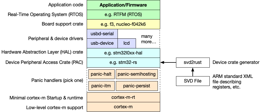
On top of the low level crates, you have PAC (peripheral access crates) and HAL (hardware abstraction layer) crates that expose access to individual peripherals in the chip. This project uses the stm32l4xx-hal crate for the HAL, which in turn is built upon the stm32l4 PAC.
I will omit the details of how Rust handles programming for bare metal embedded systems as there is already a ton of great resources out there that covers this topic in great detail. In particular, I want to callout The Embedded Rust Book as an excellent overview, followed by this document for an explanation of the internal structure of the PAC and HAL crates. There are also a number of excellent articles that provide a great overview and examples and templates on how to write a bare metal firmware in Rust.
Debugging Setup for the NUCLEO-L432KC
My development environment is a bit unique as my firmware development is done in WSL2 running Ubuntu 20.04.1 LTS. My IDE of choice however, is Visual Studio Code running on Windows while being connect to WSL via it’s remote workspace feature. This setup is a bit complicated as WSL doesn’t have direct access to the development board due to USB passthrough limitations. To work around this, the OpenOCD server needs to run on the Windows side and GDB/VSCode will have to connect to the OpenOCD server via a local network socket.
Here are the instructions on how to setup a hardware debugging session targeting the NUCLEO-L432KC development board. Instructions for targeting the Nixie clock itself will be provided later as there are a few additional steps due to the external ST-LINK/J-LINK debugger.
- Download and extract precompiled OpenOCD binaries from xPack project
- On the Windows side, run OpenOCD targeting the STM32L4 and bind to a local IP address. Note that binding to
localhostor127.0.0.1won’t work here due to WSL limitations. The binding address should be either0.0.0.0or the local IP address of a local network adapter, which in my case is10.3.0.19.1bin\openocd.exe -f interface/stlink.cfg -f target/stm32l4x.cfg -c "bindto 10.3.0.19" - In WSL, install gdb-multiarch:
1sudo apt install gdb-multiarch
- Run gdb-multiarch and target the firmware binary:
1gdb-multiarch -q target/thumbv7em-none-eabihf/debug/nixie-clock-in-8
- Connect GDB to the remote OpenOCD server:
1(gdb) target extended-remote 10.3.0.19:3333
- OpenOCD should output the following once GDB has connected:
123456789101112131415161718xPack OpenOCD, x86_64 Open On-Chip Debugger 0.11.0-00155-ge392e485e (2021-03-15-16:44)Licensed under GNU GPL v2For bug reports, readhttp://openocd.org/doc/doxygen/bugs.htmlInfo : auto-selecting first available session transport "hla_swd". To override use 'transport select <transport>'.Info : The selected transport took over low-level target control. The results might differ compared to plain JTAG/SWDInfo : Listening on port 6666 for tcl connectionsInfo : Listening on port 4444 for telnet connectionsInfo : clock speed 500 kHzInfo : STLINK V2J29M18 (API v2) VID:PID 0483:374BInfo : Target voltage: 3.257592Info : stm32l4x.cpu: hardware has 6 breakpoints, 4 watchpointsInfo : starting gdb server for stm32l4x.cpu on 3333Info : Listening on port 3333 for gdb connectionsInfo : accepting 'gdb' connection on tcp/3333Info : device idcode = 0x10016435 (STM32L43/L44xx - Rev Z : 0x1001)Info : flash size = 256kbytesInfo : flash mode : single-bank
- Load the firmware, enable semihosting, and start stepping through the firmware:
12345(gdb) load(gdb) monitor arm semihosting enable(gdb) break main(gdb) continue(gdb) step
- Note that the above commands is also in
openocd.gdb, but you will need to manually update the remote address in the script before running it.1gdb-multiarch -x openocd.gdb target/thumbv7em-none-eabihf/debug/nixie-clock-in-8 - To use VSCode’s built in debugger, the Cortex-Debug extension must first be installed. The following configuration block can then be added to launch.json to configure access to the external OpenOCD server:
123456789101112{"type": "cortex-debug","request": "launch","name": "Debug (gdb-remote)","servertype": "external","cwd": "${workspaceRoot}","preLaunchTask": "Cargo Build (debug)","runToMain": true,"executable": "./target/thumbv7em-none-eabihf/debug/nixie-clock-in-8","gdbTarget": "10.3.0.19:3333","gdbPath": "/usr/bin/gdb-multiarch"}
Debugging Setup for the Custom PCB
Unlike the NUCLEO-L432KC development board, my custom PCB doesn’t contain a built in ST-LINK in-circuit debugger/programmer so an external programmer such as the SEGGER J-Link or ST-LINK alternative is required. A debugger isn’t strictly necessary however, as the firmware on the device can be flashed directly via DFU over USB.
Rev. B of the PCB design had a Tag-Connect port to enable debugging and programming via SWD, but for some unknown reason I couldn’t get it working with either a ST-LINK or J-Link debugger. I’m not sure why this is the case as I do remember that this debug connection was working at some point. The location of the Tag-Connect was also choosen poorly as the DS3231 IC partially blocks the through hole ports used by the connector, making it so that I couldn’t use a retaining clip to hold the connector in place. In hindsight, a Mini SWD connector would have made things a lot easier while taking up almost the same amount of board space.
Bare Metal Rust Firmware
The Rust version of the clock firmware is nearly identical to the C version in terms of functionality and behavior. For comparison, the C version of the firmware is around ~1150 lines of code (not including the Mbed libraries) and compiles to a 72kB firmware binary. The Rust codebase on the other hand is a bit more verbose at ~1450 lines of code but compiles down to a tiny 14kB firmware binary.
The above isn’t a really good comparison though, as the Mbed library and runtime adds a significant amount of overhead to facilitate ease of use. Comparing the Rust implementation against one that uses CMSIS or STM32Cube would help provide better insight into exactly how much extra overhead is introduced by using Rust over C.
|
1 2 3 4 5 6 7 8 9 10 11 12 13 14 15 16 17 18 19 20 21 22 23 24 25 26 27 28 29 30 31 32 33 34 35 36 37 38 39 40 41 42 43 44 45 46 47 48 49 50 51 52 53 54 55 56 57 58 59 60 61 62 63 64 65 66 67 68 69 70 71 72 73 74 75 76 77 78 79 80 81 82 83 84 85 86 87 88 89 90 91 92 93 94 95 96 97 98 99 100 101 102 103 104 105 106 107 108 109 110 111 112 113 114 115 116 117 118 119 120 121 122 123 124 125 126 127 128 129 130 131 132 133 134 135 136 137 138 139 140 141 142 143 144 145 146 147 148 149 150 151 152 153 154 155 156 157 158 159 160 161 162 163 164 165 166 167 168 169 170 171 172 173 174 175 176 177 178 179 180 181 182 183 184 185 186 187 188 189 190 191 192 193 194 195 196 197 198 199 200 201 202 203 204 205 206 207 208 209 210 211 212 213 214 215 216 217 218 219 220 221 222 223 224 225 226 227 228 229 230 231 232 233 234 235 236 237 238 239 240 241 242 243 244 245 246 247 248 249 250 251 252 253 254 255 256 257 258 259 260 261 262 263 264 265 266 267 268 269 270 271 272 273 274 275 276 277 278 279 280 281 282 283 284 285 286 287 288 289 290 291 292 293 294 295 296 297 298 299 300 301 302 303 304 305 306 307 308 309 310 311 312 313 314 315 316 317 318 319 320 321 322 323 324 325 326 327 328 329 330 331 332 333 334 335 336 337 338 339 340 341 342 343 344 345 346 347 348 349 350 351 352 353 354 355 356 357 358 359 360 361 362 363 364 365 366 367 368 369 370 371 372 373 374 375 376 377 378 379 380 381 382 383 384 385 386 387 388 389 390 391 392 393 394 395 396 397 398 399 400 401 402 403 404 405 406 407 408 409 410 411 412 413 414 415 416 417 418 419 420 421 422 423 424 425 426 427 428 429 430 431 432 433 434 435 436 437 438 439 440 441 442 443 444 445 446 447 448 449 450 451 452 453 454 455 456 457 458 459 460 461 462 463 464 465 466 467 468 469 470 471 472 473 474 475 476 477 478 479 480 481 482 483 484 485 486 487 488 489 490 491 492 493 494 495 496 497 498 499 500 501 502 503 504 505 506 507 508 509 510 511 512 513 514 515 516 517 518 519 520 521 522 523 524 525 526 527 528 529 530 531 532 533 534 535 536 537 538 539 540 541 542 543 544 545 546 547 548 549 550 551 552 553 554 555 556 557 558 559 560 561 562 563 564 565 566 567 568 569 570 571 572 573 574 575 576 577 578 579 580 581 582 583 584 585 586 587 588 589 590 591 592 593 |
use stm32l4xx_hal::{ prelude::{ _embedded_hal_blocking_i2c_Read, _embedded_hal_blocking_i2c_Write, _embedded_hal_blocking_i2c_WriteRead, }, }; use crate::pca9685; pub const DS3231_ADDR: u8 = 0x68; pub const TUSB322_ADDR: u8 = 0x47; pub const PCA9685_ADDR_1: u8 = 0x41; pub const PCA9685_ADDR_2: u8 = 0x42; pub const PCA9685_ADDR_3: u8 = 0x43; pub const PCA9685_ALL_CALL: u8 = 0x70; // Default enabled pub const PCA9685_SUB_CALL_1: u8 = 0x71; // Default disabled pub const PCA9685_SUB_CALL_2: u8 = 0x72; // Default disabled pub const PCA9685_SUB_CALL_3: u8 = 0x73; // Default disabled pub const DISPLAY_REFRESH_FPS: u32 = 500; pub const DIGIT_FADE_DURATION_MS: u32 = 1000; pub const CYCLE_FADE_DURATION_MS: u32 = 200; pub const CYCLE_ITERATIONS: usize = 20; pub const CYCLE_REFRESH_INTERVAL: u32 = 60; pub const CYCLE_REFRESH_VARIANCE: u32 = 30; const DOT_MIN_BRIGHTNESS: u32 = 256; const DOT_MAX_BRIGHTNESS: u32 = 640; const DOT_FADE_DURATION_US: u32 = 1_000_000; const DIGIT_MAX_BRIGHTNESS: u32 = 4096; const DIGIT_MIN_BRIGHTNESS: u32 = 0; const NUM_TUBES: usize = 4; const NUM_DIGITS: usize = 10; const MAP_DOT_ADDR: u8 = PCA9685_ADDR_2; const MAP_DOT_PIN: u8 = 15; const MAP_ADDR: usize = 0; const MAP_PIN: usize = 1; struct DigitToPin { address: u8, pin: usize, } struct PwmDriver { digit: [DigitToPin; 10], } struct PwmOutputMap { driver: [PwmDriver; 4], dot_address: u8, dot_pin: usize, } static TUBE_MAPPING: PwmOutputMap = { PwmOutputMap { driver: [ PwmDriver { digit: [ DigitToPin { address: PCA9685_ADDR_1, pin: 8, }, // Tube 0 Digit 0 DigitToPin { address: PCA9685_ADDR_1, pin: 9, }, // Tube 0 Digit 1 DigitToPin { address: PCA9685_ADDR_1, pin: 10, }, // Tube 0 Digit 2 DigitToPin { address: PCA9685_ADDR_1, pin: 12, }, // Tube 0 Digit 3 DigitToPin { address: PCA9685_ADDR_1, pin: 15, }, // Tube 0 Digit 4 DigitToPin { address: PCA9685_ADDR_1, pin: 14, }, // Tube 0 Digit 5 DigitToPin { address: PCA9685_ADDR_1, pin: 11, }, // Tube 0 Digit 6 DigitToPin { address: PCA9685_ADDR_1, pin: 0, }, // Tube 0 Digit 7 DigitToPin { address: PCA9685_ADDR_1, pin: 1, }, // Tube 0 Digit 8 DigitToPin { address: PCA9685_ADDR_1, pin: 13, }, // Tube 0 Digit 9 ], }, PwmDriver { digit: [ DigitToPin { address: PCA9685_ADDR_1, pin: 5, }, // Tube 1 Digit 0 DigitToPin { address: PCA9685_ADDR_1, pin: 6, }, // Tube 1 Digit 1 DigitToPin { address: PCA9685_ADDR_1, pin: 7, }, // Tube 1 Digit 2 DigitToPin { address: PCA9685_ADDR_1, pin: 2, }, // Tube 1 Digit 3 DigitToPin { address: PCA9685_ADDR_2, pin: 4, }, // Tube 1 Digit 4 DigitToPin { address: PCA9685_ADDR_2, pin: 1, }, // Tube 1 Digit 5 DigitToPin { address: PCA9685_ADDR_1, pin: 4, }, // Tube 1 Digit 6 DigitToPin { address: PCA9685_ADDR_2, pin: 2, }, // Tube 1 Digit 7 DigitToPin { address: PCA9685_ADDR_2, pin: 3, }, // Tube 1 Digit 8 DigitToPin { address: PCA9685_ADDR_1, pin: 3, }, // Tube 1 Digit 9 ], }, PwmDriver { digit: [ DigitToPin { address: PCA9685_ADDR_3, pin: 8, }, // Tube 2 Digit 0 DigitToPin { address: PCA9685_ADDR_3, pin: 9, }, // Tube 2 Digit 1 DigitToPin { address: PCA9685_ADDR_3, pin: 10, }, // Tube 2 Digit 2 DigitToPin { address: PCA9685_ADDR_3, pin: 12, }, // Tube 2 Digit 3 DigitToPin { address: PCA9685_ADDR_2, pin: 12, }, // Tube 2 Digit 4 DigitToPin { address: PCA9685_ADDR_2, pin: 13, }, // Tube 2 Digit 5 DigitToPin { address: PCA9685_ADDR_3, pin: 11, }, // Tube 2 Digit 6 DigitToPin { address: PCA9685_ADDR_2, pin: 14, }, // Tube 2 Digit 7 DigitToPin { address: PCA9685_ADDR_2, pin: 11, }, // Tube 2 Digit 8 DigitToPin { address: PCA9685_ADDR_3, pin: 13, }, // Tube 2 Digit 9 ], }, PwmDriver { digit: [ DigitToPin { address: PCA9685_ADDR_3, pin: 5, }, // Tube 3 Digit 0 DigitToPin { address: PCA9685_ADDR_3, pin: 6, }, // Tube 3 Digit 1 DigitToPin { address: PCA9685_ADDR_3, pin: 7, }, // Tube 3 Digit 2 DigitToPin { address: PCA9685_ADDR_3, pin: 2, }, // Tube 3 Digit 3 DigitToPin { address: PCA9685_ADDR_3, pin: 14, }, // Tube 3 Digit 4 DigitToPin { address: PCA9685_ADDR_3, pin: 15, }, // Tube 3 Digit 5 DigitToPin { address: PCA9685_ADDR_3, pin: 4, }, // Tube 3 Digit 6 DigitToPin { address: PCA9685_ADDR_3, pin: 1, }, // Tube 3 Digit 7 DigitToPin { address: PCA9685_ADDR_3, pin: 0, }, // Tube 3 Digit 8 DigitToPin { address: PCA9685_ADDR_3, pin: 3, }, // Tube 3 Digit 9 ], }, ], dot_address: PCA9685_ADDR_2, dot_pin: 15, } }; #[derive(Debug, PartialEq)] enum State { Idle, Incrementing, Decrementing, } struct Digit { state: State, value: u32, pwm_start: u32, pwm_end: u32, fade_duration: Option<u32>, updated: bool, } impl Digit { const fn default() -> Self { Self { state: State::Idle, value: 0, pwm_start: 0, pwm_end: 0, fade_duration: None, updated: false, } } } struct CycleSettings { last_digit: Option<u32>, next_digit: u32, iteration: usize, last_fade_duration: u32, } struct Tube { digits: [Digit; NUM_DIGITS], last_digit: Option<u32>, cycle: Option<CycleSettings>, } impl Tube { const fn default() -> Self { const DIGIT_INIT: Digit = Digit::default(); Self { digits: [DIGIT_INIT; 10], last_digit: None, cycle: None, } } fn fade_in_out_digit(&mut self, digit: Option<u32>, fade_duration: u32, cycle_cmd: bool) { // If the tube is in the middle of a cycle sequence and a call comes // in to update the tube digit (for time), override the last value of // the cycle sequence with the new digit. if let Some(ref mut cycle) = self.cycle { if !cycle_cmd { cycle.last_digit = digit; cycle.last_fade_duration = fade_duration; } } // Dont update if actively cycling tube unless cycle_cmd is set if (self.cycle.is_none() && !cycle_cmd) || cycle_cmd { // Fade out all digits for digit in 0..NUM_DIGITS { self.digits[digit].state = State::Decrementing; self.digits[digit].fade_duration = Some(fade_duration); } // Fade in the specified digit if let Some(digit) = digit { self.digits[digit as usize].state = State::Incrementing; self.digits[digit as usize].fade_duration = Some(fade_duration); } self.last_digit = digit; } } } pub struct Clock { tubes: [Tube; NUM_TUBES], dot: Digit, minute: Option<u32>, hour: Option<u32>, } impl Clock { pub const fn default() -> Self { const TUBE_INIT: Tube = Tube::default(); Self { tubes: [TUBE_INIT; NUM_TUBES], dot: Digit::default(), minute: None, hour: None, } } // Sets a new time to be displayed pub fn rtc_tick(&mut self, second: u32, minute: u32, hour: u32) { // Update digit for each tube if value has changed match self.hour { Some(prev_hour) if prev_hour / 10 == hour / 10 => { if hour / 10 == 0 { self.tubes[0].fade_in_out_digit(None, DIGIT_FADE_DURATION_MS, false); } } _ => { self.tubes[0].fade_in_out_digit(Some(hour / 10), DIGIT_FADE_DURATION_MS, false); } } match self.hour { Some(prev_hour) if prev_hour % 10 == hour % 10 => {} _ => { self.tubes[1].fade_in_out_digit(Some(hour % 10), DIGIT_FADE_DURATION_MS, false); } } match self.minute { Some(prev_minute) if prev_minute / 10 == minute / 10 => {} _ => { self.tubes[2].fade_in_out_digit(Some(minute / 10), DIGIT_FADE_DURATION_MS, false); } } match self.minute { Some(prev_minute) if prev_minute % 10 == minute % 10 => {} _ => { self.tubes[3].fade_in_out_digit(Some(minute % 10), DIGIT_FADE_DURATION_MS, false); } } #[cfg(test)] println!( "RTC tick: {}{}:{}{}", hour / 10, hour % 10, minute / 10, minute % 10 ); // Set fade direction for dot self.dot.state = match second % 2 { 0 => State::Incrementing, 1 => State::Decrementing, _ => State::Idle, }; self.dot.fade_duration = Some(DIGIT_FADE_DURATION_MS); #[cfg(test)] println!("RTC tick: dot state is {:?}", self.dot.state); // Store the last set value for the next update self.hour = Some(hour); self.minute = Some(minute); } // Updates the display with values due to fade in/out // Returns true if values have changed pub fn fps_tick(&mut self) -> bool { let mut pending_refresh: bool = false; let mut update_fn = |digit: &mut Digit, min: u32, max: u32, steps: u32| { match digit.state { State::Incrementing => { if digit.value >= max { digit.value = max; digit.state = State::Idle; } else { digit.value = digit.value.saturating_add(steps).clamp(min, max); digit.updated = true; pending_refresh = true; } } State::Decrementing => { if digit.value <= min { digit.value = min; digit.state = State::Idle; } else { digit.value = digit.value.saturating_sub(steps).clamp(min, max); digit.updated = true; pending_refresh = true; } } State::Idle => { digit.fade_duration = None; } }; }; #[cfg(not(test))] self.tubes.iter_mut().for_each(|tube| { tube.digits.iter_mut().for_each(|digit| { if let Some(fade_duration) = digit.fade_duration { let ticks = fade_duration * 1000 / (1000 / DISPLAY_REFRESH_FPS * 1000); let steps = ((DIGIT_MAX_BRIGHTNESS - DIGIT_MIN_BRIGHTNESS) + ticks - 1) / ticks; update_fn(digit, DIGIT_MIN_BRIGHTNESS, DIGIT_MAX_BRIGHTNESS, steps); } }); }); #[cfg(test)] for (t, tube) in self.tubes.iter_mut().enumerate() { for (d, digit) in tube.digits.iter_mut().enumerate() { if let Some(fade_duration) = digit.fade_duration { let ticks = fade_duration * 1000 / (1000 / DISPLAY_REFRESH_FPS * 1000); let steps = ((DIGIT_MAX_BRIGHTNESS - DIGIT_MIN_BRIGHTNESS) + ticks - 1) / ticks; update_fn(digit, DIGIT_MIN_BRIGHTNESS, DIGIT_MAX_BRIGHTNESS, steps); } if digit.updated { println!( "Refresh tick: updated tube {} digit {} to value {}", t, d, digit.value ); } } } // Update dot values if let Some(fade_duration) = self.dot.fade_duration { let ticks = fade_duration * 1000 / (1000 / DISPLAY_REFRESH_FPS * 1000); let steps = ((DOT_MAX_BRIGHTNESS - DOT_MIN_BRIGHTNESS) + ticks - 1) / ticks; update_fn(&mut self.dot, DOT_MIN_BRIGHTNESS, DOT_MAX_BRIGHTNESS, steps); } #[cfg(test)] if self.dot.updated { println!("Refresh tick: updated dot to value {}", self.dot.value); } // Compute actual PWM values if display values have changed if pending_refresh { self.distribute_pwm(); } pending_refresh } // Updates the digit displayed during a cycle sequence // Returns true if the cycle sequence has completed pub fn cycle_tick(&mut self) -> bool { let mut cycle_ended = true; self.tubes.iter_mut().for_each(|tube| { if let Some(cycle) = tube.cycle.as_mut() { #[cfg(test)] println!("Cycle tick: iteration {}", cycle.iteration); if cycle.iteration > 0 { let next_digit = cycle.next_digit; cycle.next_digit = if cycle.next_digit == 9 { 0 } else { cycle.next_digit + 1 }; cycle.iteration = cycle.iteration - 1; tube.fade_in_out_digit(Some(next_digit), CYCLE_FADE_DURATION_MS, true); cycle_ended = false; } else { let last_digit = cycle.last_digit; let last_fade = cycle.last_fade_duration; tube.cycle = None; tube.fade_in_out_digit(last_digit, last_fade, false); } } }); cycle_ended } // Start cycling sequence for the given tube to prevent long term damage from cathode poisoning pub fn cycle_start(&mut self, tube: usize) { self.tubes[tube].cycle = Some(CycleSettings { last_digit: self.tubes[tube].last_digit, next_digit: 0, iteration: CYCLE_ITERATIONS, last_fade_duration: DIGIT_FADE_DURATION_MS, }); } // Writes updated PWM values to each PCA9685 pub fn write_i2c<T>(&mut self, i2c: &mut T) where T: _embedded_hal_blocking_i2c_WriteRead + _embedded_hal_blocking_i2c_Read + _embedded_hal_blocking_i2c_Write, { for (t, tube) in self.tubes.iter_mut().enumerate() { for (d, digit) in tube.digits.iter_mut().enumerate() { if digit.updated { pca9685::set_digit( i2c, TUBE_MAPPING.driver[t].digit[d].address, TUBE_MAPPING.driver[t].digit[d].pin, digit.pwm_start, digit.pwm_end, ); digit.updated = false; } } } if self.dot.updated { pca9685::set_digit( i2c, TUBE_MAPPING.dot_address, TUBE_MAPPING.dot_pin, self.dot.pwm_start, self.dot.pwm_end, ); self.dot.updated = false; } } // In the event that there are multiple PWM outputs at less than 100% duty cycle, // stagger the start time of each PWM to reduce the switch on surge current. If the // duty cycle is greater than 100%, distribute the PWM outputs as much as possible // to keep the current consumption at a minimum. fn distribute_pwm(&mut self) { let mut last_pwm: u32 = 0; let mut incrementing: bool = true; // Closure to avoid duplicate code let mut update_digit = |digit: &mut Digit| { if digit.value == DIGIT_MIN_BRIGHTNESS { digit.pwm_start = 0; digit.pwm_end = 0; } else if digit.value == DIGIT_MAX_BRIGHTNESS { digit.pwm_start = 0; digit.pwm_end = DIGIT_MAX_BRIGHTNESS; } else { if incrementing { if last_pwm + digit.value > DIGIT_MAX_BRIGHTNESS { digit.pwm_start = DIGIT_MAX_BRIGHTNESS - digit.value; digit.pwm_end = DIGIT_MAX_BRIGHTNESS; last_pwm = digit.pwm_start; incrementing = false; } else { digit.pwm_start = last_pwm; digit.pwm_end = digit.pwm_start + digit.value; last_pwm = digit.pwm_end; } } else { if last_pwm - DIGIT_MIN_BRIGHTNESS < digit.value { digit.pwm_start = DIGIT_MIN_BRIGHTNESS; digit.pwm_end = digit.pwm_start + digit.value; last_pwm = digit.pwm_end; incrementing = true; } else { digit.pwm_end = last_pwm; digit.pwm_start = digit.pwm_end - digit.value; last_pwm = digit.pwm_start; } } digit.updated = true; } }; #[cfg(not(test))] self.tubes.iter_mut().for_each(|tube| { tube.digits.iter_mut().for_each(|digit| { update_digit(digit); }); }); #[cfg(test)] for (t, tube) in self.tubes.iter_mut().enumerate() { for (d, digit) in tube.digits.iter_mut().enumerate() { update_digit(digit); if digit.updated { println!( "Distribute PWM: tube {} digit {} start {} end {}", t, d, digit.pwm_start, digit.pwm_end ); } } } // The dot is somewhat sensitive to changes to PWM signal, so for the sake // of consistency, keep the signal on time at the end of the PWM period. // Otherwise the distribution algorithm will sometimes place the on time at // the end of the PWM period in one cycle and at the start of the period for // the next, which results in visual flickers. // update_digit(&mut self.dot); self.dot.pwm_start = DIGIT_MAX_BRIGHTNESS - self.dot.value; self.dot.pwm_end = DIGIT_MAX_BRIGHTNESS; #[cfg(test)] println!( "Distribute PWM: dot start {} end {}", self.dot.pwm_start, self.dot.pwm_end ); } } #[cfg(test)] mod test { use super::*; use std::println; #[test] fn pwm_calc_test() { let mut clock: Clock = Clock::default(); // Initialize clock to arbitrary time clock.rtc_tick(10, 8, 12); // Iterate and print output values for each display refresh tick for tick in 0..1000 { println!("\nRefresh tick: {}", tick); if !clock.fps_tick() { println!("Refresh halted"); break; } // Reset the updated field for each digit clock.tubes.iter_mut().for_each(|tube| { tube.digits.iter_mut().for_each(|digit| { digit.updated = false; }); }); clock.dot.updated = false; } } #[test] fn cycle_test() { let mut clock: Clock = Clock::default(); // Initialize clock to arbitrary time clock.rtc_tick(00, 27, 8); // Simulate a cycle refresh sequence on tube 0 clock.tubes[0].cycle = Some(CycleSettings { last_digit: clock.tubes[0].last_digit, next_digit: 0, iteration: CYCLE_ITERATIONS, last_fade_duration: DIGIT_FADE_DURATION_MS, }); // Iterate and print debug values for each cycle for cycle in 0..1000 { println!("\nCycle tick: {}", cycle); if clock.cycle_tick() { println!("Cycle halted"); break; } // Iterate and print output values for each display refresh tick for tick in 0..1000 { println!("\nRefresh tick: {}", tick); if !clock.fps_tick() { println!("Refresh halted"); break; } // Reset the updated field for each digit clock.tubes.iter_mut().for_each(|tube| { tube.digits.iter_mut().for_each(|digit| { digit.updated = false; }); }); clock.dot.updated = false; } } } } |
The ability to run unit tests on the host PC proved to be far more useful that I originally thought. The project itself normally targets the thumbv7em-none-eabihf architecture for the Cortex-M4F on the STM32F432KC, but it’s actually possible to structure the tests such that they run on the host architecture. I took advantage of this in my code to enable validation of most of the internal logic without having to push a new firmware to the device for each change. An example would be running the following to simulate and print the calculated output of each digit for each nixie tube for every frame refresh of the display:
|
1 |
cargo test --target=x86_64-unknown-linux-gnu nixie::test::cycle_test -- --show-output |
The Rust firmware that I wrote actually comes in two variations, one that builds on the cortex-m-rt crate and one that uses the Real-Time Interrupt-driven Concurrency framework (cortex-m-rtic). The RTIC framework makes it incredibly easy to setup and safely utilize interrupts, with support for asynchronous tasks, efficient interrupt prioritization, and guaranteed deadlock free execution. The drawback is that the compile time errors can be quite hard to decipher due to the extensive use of macros by this framework.
The initialization code is nearly identical between the two versions, with most of the difference being in how the interrupts and static peripherals are defined. The RTIC implementation adds an extra overhead of 632 bytes, resulting in a firmware size of 14400 bytes compared to the 13768 bytes of the non-RTIC version.
Minimal Runtime
|
1 2 3 4 5 6 7 8 9 10 11 12 13 14 15 16 17 18 19 20 21 22 23 24 25 26 27 28 29 30 31 32 33 34 35 36 37 38 39 40 41 42 43 44 45 46 47 48 49 50 51 52 53 54 55 56 57 58 59 60 61 62 63 64 65 66 67 68 69 70 71 72 73 74 75 76 77 78 79 80 81 82 83 84 85 86 87 88 89 90 91 92 93 94 95 96 97 98 99 100 101 102 103 104 105 106 107 108 109 110 111 112 113 114 115 116 117 118 119 120 121 122 123 124 125 126 127 128 129 130 131 132 133 134 135 136 137 138 139 140 141 142 143 144 145 146 147 148 149 150 151 152 153 154 155 156 157 158 159 160 161 162 163 164 165 166 167 168 169 170 171 172 173 174 175 176 177 178 179 180 181 182 183 184 185 186 187 188 189 190 191 192 193 194 195 196 197 198 199 200 201 202 203 204 205 206 207 208 209 210 211 212 213 214 215 216 217 218 219 220 221 222 223 224 225 226 227 228 229 230 231 232 233 234 235 236 237 238 239 240 241 242 243 244 245 246 247 248 249 250 251 252 253 254 255 256 257 258 259 260 261 262 263 264 265 266 267 268 269 270 271 272 273 274 275 276 277 278 279 280 281 282 283 284 285 286 287 288 289 290 291 292 293 294 295 296 297 298 299 300 301 302 303 304 305 306 307 308 309 310 311 312 313 314 315 316 317 318 319 320 321 322 323 324 325 326 327 328 329 330 331 332 333 334 335 336 337 338 339 340 341 342 343 344 345 346 347 348 349 350 351 |
#![cfg_attr(test, allow(unused_imports))] #![cfg_attr(not(test), no_std)] #![cfg_attr(not(test), no_main)] #![feature(half_open_range_patterns)] #![feature(exclusive_range_pattern)] #![allow(dead_code)] // custom panic handler #[cfg(not(test))] use core::panic::PanicInfo; use core::{cell::RefCell, ops::DerefMut}; use cortex_m::{interrupt::free, interrupt::Mutex, peripheral::NVIC}; use cortex_m_rt::entry; use stm32l4xx_hal::{delay::Delay, device::{I2C1, TIM2, TIM7}, gpio::{ Alternate, Edge, Floating, Input, OpenDrain, Output, PullUp, PushPull, AF4, PA3, PB5, PC15, }, gpio::{State, PA10, PA9}, i2c::I2c, interrupt, pac, prelude::*, rcc, stm32::Interrupt, timer::{Timer, Event}, }; mod ds3231; mod nixie; mod pca9685; mod tusb322; use nixie::*; // Local peripheral mappings type RtcInt = PB5<Input<Floating>>; type FaultInt = PA3<Input<PullUp>>; type FaultLed = PC15<Output<PushPull>>; type I2c1 = I2c<I2C1, (PA9<Alternate<AF4, Output<OpenDrain>>>,PA10<Alternate<AF4,Output<OpenDrain>>>)>; type FpsTimer = Timer<TIM2>; type CycleTimer = Timer<TIM7>; // Global peripheral singletons static RTC_INT: Mutex<RefCell<Option<RtcInt>>> = Mutex::new(RefCell::new(None)); static FAULT_INT: Mutex<RefCell<Option<FaultInt>>> = Mutex::new(RefCell::new(None)); static FAULT_LED: Mutex<RefCell<Option<FaultLed>>> = Mutex::new(RefCell::new(None)); static I2C: Mutex<RefCell<Option<I2c1>>> = Mutex::new(RefCell::new(None)); static REFRESH_TIMER: Mutex<RefCell<Option<FpsTimer>>> = Mutex::new(RefCell::new(None)); static CYCLE_TIMER: Mutex<RefCell<Option<CycleTimer>>> = Mutex::new(RefCell::new(None)); static CLOCK: Mutex<RefCell<Clock>> = Mutex::new(RefCell::new(Clock::default())); #[cfg(not(test))] #[entry] fn main() -> ! { // Acquire a singleton instance for the chip's peripherals let mut dp = pac::Peripherals::take().unwrap(); let cp = pac::CorePeripherals::take().unwrap(); // Consume the raw peripheral and return a new object that implements a higher level API let mut flash = dp.FLASH.constrain(); let mut rcc = dp.RCC.constrain(); let mut pwr = dp.PWR.constrain(&mut rcc.apb1r1); // Configure clocks to run at maximum frequency off internal oscillator let clocks = rcc .cfgr .pll_source(rcc::PllSource::HSI16) .sysclk(64.mhz()) .hclk(64.mhz()) .pclk1(64.mhz()) .pclk2(64.mhz()) .hsi48(true) .freeze(&mut flash.acr, &mut pwr); // Configure delay timer that operates off systick timer let mut delay_timer = Delay::new(cp.SYST, clocks); // Split GPIO peripheral into independent pins and registers let mut gpioa = dp.GPIOA.split(&mut rcc.ahb2); let mut gpiob = dp.GPIOB.split(&mut rcc.ahb2); let mut gpioc = dp.GPIOC.split(&mut rcc.ahb2); // Configure high voltage PSU enable pin on PA2 let mut hv_enable = gpioa.pa2.into_push_pull_output_with_state(&mut gpioa.moder, &mut gpioa.otyper, State::Low); // Configure serial port // let tx = gpiob.pb6.into_af7(&mut gpiob.moder, &mut gpiob.afrl); // let rx = gpiob.pb7.into_af7(&mut gpiob.moder, &mut gpiob.afrl); // let _serial = Serial::usart1( // dp.USART1, // (tx, rx), // Config::default().baudrate(115_200.bps()), // clocks, // &mut rcc.apb2, // ); // Configure fault LED output on PC15 let fault_led = gpioc.pc15.into_push_pull_output_with_state(&mut gpioc.moder, &mut gpioc.otyper, State::Low); // Store fault LED in static singleton so that it's accessible from anywhere free(|cs| { FAULT_LED.borrow(cs).replace(Some(fault_led)); }); // Configure fault input interrupt on PA3 let mut fault_int = gpioa.pa3.into_pull_up_input(&mut gpioa.moder, &mut gpioa.pupdr); fault_int.make_interrupt_source(&mut dp.SYSCFG, &mut rcc.apb2); fault_int.enable_interrupt(&mut dp.EXTI); fault_int.trigger_on_edge(&mut dp.EXTI, Edge::FALLING); // Sanity check that fault pin isn't already set (active low) before enabling interrupt if fault_int.is_high().unwrap() { // Configure NVIC mask to enable interrupt source unsafe { NVIC::unmask(Interrupt::EXTI3); } // Store fault interrupt in static singleton so that interrupt has access to it free(|cs| { FAULT_INT.borrow(cs).replace(Some(fault_int)); }); } else { panic!(); } // Enable RNG peripheral let rng = dp.RNG.enable(&mut rcc.ahb2, clocks); // Configure I2C SCL pin let scl = gpioa.pa9.into_open_drain_output(&mut gpioa.moder, &mut gpioa.otyper); let scl = scl.into_af4(&mut gpioa.moder, &mut gpioa.afrh); // Configure I2C SDA pin let sda = gpioa.pa10.into_open_drain_output(&mut gpioa.moder, &mut gpioa.otyper); let sda = sda.into_af4(&mut gpioa.moder, &mut gpioa.afrh); // Initialize I2C (configured for 1Mhz, but actually runs at 600kHz) let mut i2c = I2c::i2c1(dp.I2C1, (scl, sda), 1.mhz(), clocks, &mut rcc.apb1r1); // Initialize TUSB322 (USB Type-C configuration chip) tusb322::init(TUSB322_ADDR, &mut i2c); // Initialize DS3231 (RTC) ds3231::init(DS3231_ADDR, &mut i2c); // ds3231::set_date(DS3231_ADDR, &mut i2c, ds3231::Weekday::Wednesday, 15, 9, 21, 20); // ds3231::set_time(DS3231_ADDR, &mut i2c, 00, 37, 12); // Configure input interrupt pin from DS3231 on PB5 // Interrupt is pulled high, with open drain on DS3231 let mut rtc_int = gpiob.pb5.into_floating_input(&mut gpiob.moder, &mut gpiob.pupdr); rtc_int.make_interrupt_source(&mut dp.SYSCFG, &mut rcc.apb2); rtc_int.enable_interrupt(&mut dp.EXTI); rtc_int.trigger_on_edge(&mut dp.EXTI, Edge::FALLING); // Configure NVIC mask to enable interrupt from DS3231 unsafe { NVIC::unmask(Interrupt::EXTI9_5); } // Store RTC interrupt in static singleton so that interrupt has access to it free(|cs| { RTC_INT.borrow(cs).replace(Some(rtc_int)); }); // Configure DAC AMP enable pin for AD8591 on PB1 let mut _dac_enable = gpiob.pb1.into_push_pull_output_with_state(&mut gpiob.moder, &mut gpiob.otyper, State::High); // Configure DAC VIN for AD8591 on PA5 // Note that this pin should actually be configured as analog output (for DAC) // but stm32l4xx_hal doesn't have support for the DAC as of now. We also currently // set the output to only the highest possible voltage, so the same functionality // can be achieved by configuring the pin as a digital output set to high. let mut _dac_output = gpioa.pa5.into_push_pull_output_with_state(&mut gpioa.moder, &mut gpioa.otyper, State::High); // Configure PWM enable pin (active low) for PCA9685 on PA7 let mut pwm_enable = gpioa.pa7.into_push_pull_output_with_state(&mut gpioa.moder, &mut gpioa.otyper, State::High); // Initialize the PCA9685 display refresh timer let refresh_timer = Timer::tim2(dp.TIM2, nixie::DISPLAY_REFRESH_FPS.hz(), clocks, &mut rcc.apb1r1); // Configure NVIC mask to enable interrupt for the display refresh timer unsafe { NVIC::unmask(Interrupt::TIM2) }; // Save display refresh timer in static singleton so that interrupt has access to it free(|cs| { REFRESH_TIMER.borrow(cs).replace(Some(refresh_timer)); }); // Initiaize display cycle timer let cycle_timer = Timer::tim7(dp.TIM7, (1000 / nixie::CYCLE_FADE_DURATION_MS).hz(), clocks, &mut rcc.apb1r1); // Configure NVIC mask to enable interrupt for display cycle timer unsafe { NVIC::unmask(Interrupt::TIM7) }; // Save display cycle timer in static singleton so that interrupt has access to it free(|cs| { CYCLE_TIMER.borrow(cs).replace(Some(cycle_timer)); }); // Small delay to ensure that PCA9685 is fully powered on before writing to it delay_timer.delay_us(10_u32); // Initialize PCA9685 (PWM driver) pca9685::init(PCA9685_ALL_CALL, &mut i2c); // Enable PWM output after PCA9685 has been initialized pwm_enable.set_low().unwrap(); // Store I2C peripheral in global static variable as it is used in interrupt free(|cs| { I2C.borrow(cs).replace(Some(i2c)); }); // Enable the high voltage power supply last hv_enable.set_high().unwrap(); // Cycle through all tubes on powerup start_cycle(0); start_cycle(1); start_cycle(2); start_cycle(3); loop { // Delay before cycling digits to prevent cathode poisoning delay_timer.delay_ms(CYCLE_REFRESH_INTERVAL * 1000); // Choose a random tube to cycle let tube = (rng.get_random_data() % 4) as usize; start_cycle(tube); } } // Trigger the start of a new cycle sequence fn start_cycle(tube: usize) { free(|cs| { let mut cycle_timer_ref = CYCLE_TIMER.borrow(cs).borrow_mut(); let mut clock_ref = CLOCK.borrow(cs).borrow_mut(); if let Some(ref mut cycle_timer) = cycle_timer_ref.deref_mut() { // Trigger the start of a cycling sequence clock_ref.deref_mut().cycle_start(tube); // Start the timer to cycle through individual digits cycle_timer.listen(Event::TimeOut); } }); } // Interrupt handler for 1HZ signal from offchip RTC (DS3231) #[interrupt] fn EXTI9_5() { free(|cs| { let mut rtc_int_ref = RTC_INT.borrow(cs).borrow_mut(); let mut i2c_int_ref = I2C.borrow(cs).borrow_mut(); let mut refresh_timer_ref = REFRESH_TIMER.borrow(cs).borrow_mut(); let mut clock_ref = CLOCK.borrow(cs).borrow_mut(); if let Some(ref mut rtc_int) = rtc_int_ref.deref_mut() { if let Some(ref mut i2c) = i2c_int_ref.deref_mut() { if let Some(ref mut refresh_timer) = refresh_timer_ref.deref_mut() { // Read new time from DS3231 let (second, minute, hour) = ds3231::get_time(DS3231_ADDR, i2c); let (weekday, day, month, _, _) = ds3231::get_date(DS3231_ADDR, i2c); // Calculate new values and account for DST let hour = if ds3231::in_dst(weekday, day, month, hour) { (hour + 1) % 12 } else { hour % 12 }; let hour = if hour == 0 { 12 } else { hour }; // Trigger the processing of a new time value clock_ref.deref_mut().rtc_tick(second, minute, hour); // Start the refresh timer to update the display refresh_timer.listen(Event::TimeOut); // Clear the interrupt flag for the timer rtc_int.clear_interrupt_pending_bit(); } } } }); } // Interrupt handler for fault interrupt from USB monitor (TUSB322) #[interrupt] fn EXTI3() { free(|cs| { let mut nfault_ref = FAULT_INT.borrow(cs).borrow_mut(); if let Some(ref mut nfault) = nfault_ref.deref_mut() { if nfault.check_interrupt() { nfault.clear_interrupt_pending_bit(); panic!(); } } }); } // Interrupt handler for internal timer that drives display refresh rate #[interrupt] fn TIM2() { free(|cs| { let mut i2c_int_ref = I2C.borrow(cs).borrow_mut(); let mut refresh_timer_ref = REFRESH_TIMER.borrow(cs).borrow_mut(); let mut clock_ref = CLOCK.borrow(cs).borrow_mut(); if let Some(ref mut i2c) = i2c_int_ref.deref_mut() { if let Some(ref mut refresh_timer) = refresh_timer_ref.deref_mut() { // Write new values if values have changed, otherwise disable the refresh timer if clock_ref.deref_mut().fps_tick() { clock_ref.deref_mut().write_i2c(i2c); refresh_timer.clear_interrupt(Event::TimeOut); } else { refresh_timer.unlisten(Event::TimeOut); } } } }); } // Interrupt handler for internal timer that drives individual digits within a cycle sequence #[interrupt] fn TIM7() { free(|cs| { let mut cycle_timer_ref = CYCLE_TIMER.borrow(cs).borrow_mut(); let mut refresh_timer_ref = REFRESH_TIMER.borrow(cs).borrow_mut(); let mut clock_ref = CLOCK.borrow(cs).borrow_mut(); if let Some(ref mut cycle_timer) = cycle_timer_ref.deref_mut() { if let Some(ref mut refresh_timer) = refresh_timer_ref.deref_mut() { // Trigger the next step in the cycling sequence if clock_ref.deref_mut().cycle_tick() { cycle_timer.unlisten(Event::TimeOut); } else { cycle_timer.clear_interrupt(Event::TimeOut); } // Start the refresh timer to update the display refresh_timer.listen(Event::TimeOut); } } }); } // Helper function to set onboard LED state fn set_fault_led(state: State) { free(|cs| { let mut led_ref = FAULT_LED.borrow(cs).borrow_mut(); if let Some(ref mut led) = led_ref.deref_mut() { match state { State::High => led.set_high().unwrap(), State::Low => led.set_low().unwrap(), }; } }); } // Custom panic handler #[panic_handler] #[cfg(not(test))] fn panic(_info: &PanicInfo) -> ! { set_fault_led(State::High); loop { continue; } } |
Real-Time Interrupt-driven Concurrency Framework
|
1 2 3 4 5 6 7 8 9 10 11 12 13 14 15 16 17 18 19 20 21 22 23 24 25 26 27 28 29 30 31 32 33 34 35 36 37 38 39 40 41 42 43 44 45 46 47 48 49 50 51 52 53 54 55 56 57 58 59 60 61 62 63 64 65 66 67 68 69 70 71 72 73 74 75 76 77 78 79 80 81 82 83 84 85 86 87 88 89 90 91 92 93 94 95 96 97 98 99 100 101 102 103 104 105 106 107 108 109 110 111 112 113 114 115 116 117 118 119 120 121 122 123 124 125 126 127 128 129 130 131 132 133 134 135 136 137 138 139 140 141 142 143 144 145 146 147 148 149 150 151 152 153 154 155 156 157 158 159 160 161 162 163 164 165 166 167 168 169 170 171 172 173 174 175 176 177 178 179 180 181 182 183 184 185 186 187 188 189 190 191 192 193 194 195 196 197 198 199 200 201 202 203 204 205 206 207 208 209 210 211 212 213 214 215 216 217 218 219 220 221 222 223 224 225 226 227 228 229 230 231 232 233 234 235 236 237 238 239 240 241 242 243 244 245 246 247 248 249 250 251 252 253 254 255 256 257 258 259 260 261 262 263 264 265 266 267 268 269 270 271 272 273 274 275 276 277 278 279 280 281 282 283 284 285 286 287 288 289 290 291 292 293 294 295 296 297 298 299 300 301 302 303 304 305 306 307 308 309 310 311 312 313 314 315 316 317 318 319 320 321 322 323 324 325 326 |
#![cfg_attr(test, allow(unused_imports))] #![cfg_attr(not(test), no_std)] #![cfg_attr(not(test), no_main)] #![feature(half_open_range_patterns)] #![feature(exclusive_range_pattern)] #![feature(destructuring_assignment)] #![allow(dead_code)] // custom panic handler #[cfg(not(test))] use core::panic::PanicInfo; use core::{cell::RefCell, ops::DerefMut}; use cortex_m::interrupt::{Mutex, free}; use stm32l4xx_hal::{delay::Delay, device::{I2C1, TIM2, TIM7}, gpio::{ Alternate, Edge, Floating, Input, OpenDrain, Output, PullUp, PushPull, AF4, PA3, PB5, PC15, }, gpio::{State, PA10, PA9}, i2c::I2c, prelude::*, rcc, rng::Rng, timer::{Timer, Event}}; mod ds3231; mod nixie; mod pca9685; mod tusb322; use nixie::*; type FaultLed = PC15<Output<PushPull>>; static FAULT_LED: Mutex<RefCell<Option<FaultLed>>> = Mutex::new(RefCell::new(None)); #[rtic::app(device = stm32l4xx_hal::pac, peripherals = true)] const APP: () = { struct Resources { #[init(Clock::default())] clock: Clock, // Late initialized resources (shared peripherals) rtc_int: PB5<Input<Floating>>, fault_int: PA3<Input<PullUp>>, i2c: I2c<I2C1, (PA9<Alternate<AF4, Output<OpenDrain>>>,PA10<Alternate<AF4,Output<OpenDrain>>>)>, refresh_timer: Timer<TIM2>, cycle_timer: Timer<TIM7>, delay_timer: Delay, rng: Rng, } #[init(spawn = [start_cycle])] fn init(ctx: init::Context) -> init::LateResources { let mut dp = ctx.device; let cp = ctx.core; // Consume the raw peripheral and return a new object that implements a higher level API let mut flash = dp.FLASH.constrain(); let mut rcc = dp.RCC.constrain(); let mut pwr = dp.PWR.constrain(&mut rcc.apb1r1); // Configure clocks to run at maximum frequency off internal oscillator let clocks = rcc .cfgr .pll_source(rcc::PllSource::HSI16) .sysclk(64.mhz()) .hclk(64.mhz()) .pclk1(64.mhz()) .pclk2(64.mhz()) .hsi48(true) .freeze(&mut flash.acr, &mut pwr); // Configure delay timer that operates off systick timer let mut delay_timer = Delay::new(cp.SYST, clocks); // Split GPIO peripheral into independent pins and registers let mut gpioa = dp.GPIOA.split(&mut rcc.ahb2); let mut gpiob = dp.GPIOB.split(&mut rcc.ahb2); let mut gpioc = dp.GPIOC.split(&mut rcc.ahb2); // Configure high voltage PSU enable pin on PA2 let mut hv_enable = gpioa.pa2.into_push_pull_output_with_state(&mut gpioa.moder, &mut gpioa.otyper, State::Low); // Configure serial port // let tx = gpiob.pb6.into_af7(&mut gpiob.moder, &mut gpiob.afrl); // let rx = gpiob.pb7.into_af7(&mut gpiob.moder, &mut gpiob.afrl); // let _serial = Serial::usart1( // dp.USART1, // (tx, rx), // Config::default().baudrate(115_200.bps()), // clocks, // &mut rcc.apb2, // ); // Configure fault LED output on PC15 let fault_led = gpioc.pc15.into_push_pull_output_with_state(&mut gpioc.moder, &mut gpioc.otyper, State::Low); // Store fault LED in static singleton so that it's accessible from anywhere free(|cs| { FAULT_LED.borrow(cs).replace(Some(fault_led)); }); // Configure fault input interrupt on PA3 let mut fault_int = gpioa.pa3.into_pull_up_input(&mut gpioa.moder, &mut gpioa.pupdr); fault_int.make_interrupt_source(&mut dp.SYSCFG, &mut rcc.apb2); fault_int.enable_interrupt(&mut dp.EXTI); fault_int.trigger_on_edge(&mut dp.EXTI, Edge::FALLING); // Sanity check that fault pin isn't already set (active low) if fault_int.is_low().unwrap() { panic!(); } // Enable RNG peripheral let rng = dp.RNG.enable(&mut rcc.ahb2, clocks); // Configure I2C SCL pin let scl = gpioa.pa9.into_open_drain_output(&mut gpioa.moder, &mut gpioa.otyper); let scl = scl.into_af4(&mut gpioa.moder, &mut gpioa.afrh); // Configure I2C SDA pin let sda = gpioa.pa10.into_open_drain_output(&mut gpioa.moder, &mut gpioa.otyper); let sda = sda.into_af4(&mut gpioa.moder, &mut gpioa.afrh); // Initialize I2C (configured for 1Mhz, but actually runs at 600kHz) let mut i2c = I2c::i2c1(dp.I2C1, (scl, sda), 1.mhz(), clocks, &mut rcc.apb1r1); // Initialize TUSB322 (USB Type-C configuration chip) tusb322::init(TUSB322_ADDR, &mut i2c); // Initialize DS3231 (RTC) ds3231::init(DS3231_ADDR, &mut i2c); // ds3231::set_date(DS3231_ADDR, &mut i2c, ds3231::Weekday::Wednesday, 15, 9, 21, 20); // ds3231::set_time(DS3231_ADDR, &mut i2c, 00, 37, 12); // Configure input interrupt pin from DS3231 on PB5 // Interrupt is pulled high, with open drain on DS3231 // Interrupt enable is automatically handled by RTIC's #[task] let mut rtc_int = gpiob.pb5.into_floating_input(&mut gpiob.moder, &mut gpiob.pupdr); rtc_int.make_interrupt_source(&mut dp.SYSCFG, &mut rcc.apb2); rtc_int.enable_interrupt(&mut dp.EXTI); rtc_int.trigger_on_edge(&mut dp.EXTI, Edge::FALLING); // Configure DAC AMP enable pin for AD8591 on PB1 let mut _dac_enable = gpiob.pb1.into_push_pull_output_with_state(&mut gpiob.moder, &mut gpiob.otyper, State::High); // Configure DAC VIN for AD8591 on PA5 // Note that this pin should actually be configured as analog output (for DAC) // but stm32l4xx_hal doesn't have support for the DAC as of now. We also currently // set the output to only the highest possible voltage, so the same functionality // can be achieved by configuring the pin as a digital output set to high. let mut _dac_output = gpioa.pa5.into_push_pull_output_with_state(&mut gpioa.moder, &mut gpioa.otyper, State::High); // Configure PWM enable pin (active low) for PCA9685 on PA7 let mut pwm_enable = gpioa.pa7.into_push_pull_output_with_state(&mut gpioa.moder, &mut gpioa.otyper, State::High); // Initialize the PCA9685 display refresh timer // Interrupt enable is automatically handled by RTIC's #[task] let refresh_timer = Timer::tim2(dp.TIM2, nixie::DISPLAY_REFRESH_FPS.hz(), clocks, &mut rcc.apb1r1); // Initiaize display cycle timer // Interrupt enable is automatically handled by RTIC's #[task] let cycle_timer = Timer::tim7(dp.TIM7, (1000 / nixie::CYCLE_FADE_DURATION_MS).hz(), clocks, &mut rcc.apb1r1); // Small delay to ensure that PCA9685 is fully powered on before writing to it delay_timer.delay_us(10_u32); // Initialize PCA9685 (PWM driver) pca9685::init(PCA9685_ALL_CALL, &mut i2c); // Enable PWM output after PCA9685 has been initialized pwm_enable.set_low().unwrap(); // Enable the high voltage power supply last hv_enable.set_high().unwrap(); // Spawn tasks to cycle through all tubes on powerup ctx.spawn.start_cycle(0).unwrap(); ctx.spawn.start_cycle(1).unwrap(); ctx.spawn.start_cycle(2).unwrap(); ctx.spawn.start_cycle(3).unwrap(); init::LateResources { rtc_int, fault_int, i2c, refresh_timer, cycle_timer, delay_timer, rng } } #[idle(spawn = [start_cycle], resources = [delay_timer, rng])] fn idle(ctx: idle::Context) -> ! { let idle::Resources {delay_timer, rng} = ctx.resources; loop { // Delay before cycling digits to prevent cathode poisoning delay_timer.delay_ms(CYCLE_REFRESH_INTERVAL * 1000); // Choose a random tube to cycle let tube = (rng.get_random_data() % 4) as usize; ctx.spawn.start_cycle(tube).unwrap(); } } // Trigger the start of a new cycle sequence #[task(resources = [clock, cycle_timer], priority = 2, capacity = 4)] fn start_cycle(ctx: start_cycle::Context, tube: usize) { let start_cycle::Resources {mut clock, cycle_timer} = ctx.resources; // Lower priority task requires a critical section to access shared data clock.lock(|clock| { // Trigger the start of a cycling sequence clock.cycle_start(tube); }); // Start the timer to cycle through individual digits cycle_timer.listen(Event::TimeOut); } // Interrupt handler for 1HZ signal from offchip RTC (DS3231) #[task(binds = EXTI9_5, priority = 1, resources = [clock, rtc_int, i2c, refresh_timer])] fn rtc_interrupt(ctx: rtc_interrupt::Context) { let rtc_interrupt::Resources {mut clock, rtc_int, mut i2c, mut refresh_timer} = ctx.resources; let (mut second, mut minute, mut hour) = (0, 0, 0); let (mut weekday, mut day, mut month) = (ds3231::Weekday::Sunday, 0, 0); // Lower priority task requires a critical section to access shared peripheral i2c.lock(|i2c| { // Read new time from DS3231 (second, minute, hour) = ds3231::get_time(DS3231_ADDR, i2c); (weekday, day, month, ..) = ds3231::get_date(DS3231_ADDR, i2c); }); // Calculate new values and account for DST let hour = if ds3231::in_dst(weekday, day, month, hour) { (hour + 1) % 12 } else { hour % 12 }; let hour = if hour == 0 { 12 } else { hour }; // Lower priority task requires a critical section to access shared peripheral clock.lock(|clock| { // Trigger the processing of a new time value clock.rtc_tick(second, minute, hour); }); // Start the refresh timer to update the display // Lower priority task requires a critical section to access shared peripheral refresh_timer.lock(|refresh_timer| { refresh_timer.listen(Event::TimeOut); }); // Clear the interrupt flag for the timer rtc_int.clear_interrupt_pending_bit(); } // Interrupt handler for fault interrupt from USB monitor (TUSB322) // Configured as priority 4 for highest priority (pre-empts all other interrupts) #[task(binds = EXTI3, priority = 4, resources = [fault_int])] fn fault_interrupt(ctx: fault_interrupt::Context) { let fault_interrupt::Resources {fault_int} = ctx.resources; if fault_int.check_interrupt() { fault_int.clear_interrupt_pending_bit(); panic!(); } } // Interrupt handler for internal timer that drives display refresh rate #[task(binds = TIM2, priority = 3, resources = [clock, i2c, refresh_timer])] fn refresh_interrupt(ctx: refresh_interrupt::Context) { let refresh_interrupt::Resources {clock, refresh_timer, i2c} = ctx.resources; // Write new values if values have changed, otherwise disable the refresh timer if clock.fps_tick() { clock.write_i2c(i2c); refresh_timer.clear_interrupt(Event::TimeOut); } else { refresh_timer.unlisten(Event::TimeOut); } } // Interrupt handler for internal timer that drives individual digits within a cycle sequence #[task(binds = TIM7, priority = 2, resources = [clock, refresh_timer, cycle_timer])] fn cycle_interrupt(ctx: cycle_interrupt::Context) { let cycle_interrupt::Resources {mut clock, mut refresh_timer, cycle_timer} = ctx.resources; let mut cycle_ended = true; // Lower priority task requires a critical section to access shared data clock.lock(|clock| { cycle_ended = clock.cycle_tick(); }); // Trigger the next step in the cycling sequence if cycle_ended { cycle_timer.unlisten(Event::TimeOut); } else { cycle_timer.clear_interrupt(Event::TimeOut); } // Start the refresh timer to update the display // Lower priority task requires a critical section to access shared peripheral refresh_timer.lock(|refresh_timer| { refresh_timer.listen(Event::TimeOut); }); } // RTIC requires that unused interrupts are declared in an extern block when // using software tasks; these free interrupts will be used to dispatch the // software tasks. extern "C" { fn TSC(); fn LCD(); fn AES(); } }; // Helper function to set onboard LED state fn set_fault_led(state: State) { free(|cs| { let mut led_ref = FAULT_LED.borrow(cs).borrow_mut(); if let Some(ref mut led) = led_ref.deref_mut() { match state { State::High => led.set_high().unwrap(), State::Low => led.set_low().unwrap(), }; } }); } // Custom panic handler #[panic_handler] #[cfg(not(test))] fn panic(_info: &PanicInfo) -> ! { set_fault_led(State::High); loop { continue; } } |
Display Animation
Taking photos and/or videos of lit Nixie tubes is actually quite a daunting task. Due to the light emitting nature of these tubes, capturing the full dynamic range of the tubes is very difficult. The video below was taken with more dynamic range than usual (courtesy of Magic Lantern) with a significant amount of post-processing done to lower the highlights at peak brightness. Even so, the results don’t quite match what the eye sees and neither is the color reproduction particularly great..
- Cycling through all digits at 100% brightness
- Toggling digits via current modulation(~0.3mA to ~3mA)
- Toggling digits via PWM frequency (0% to 7%)
- Toggling digits via PWM frequency (0% to 100%)
- Fading through sequential digits via PWM (0% to 100%)
- Fading through random digits via PWM (0% to 100%)
- Fast cycling through sequential digits
- Fast cycling through random digits
- Initial turn-on animation (cycling through all digits)
- Clock with random digit cycling (refresh every ~10s)