The latest code base for the LED cube can be found here


12/12/2013 – Added support for controllers as well as Snake and Tron game modes
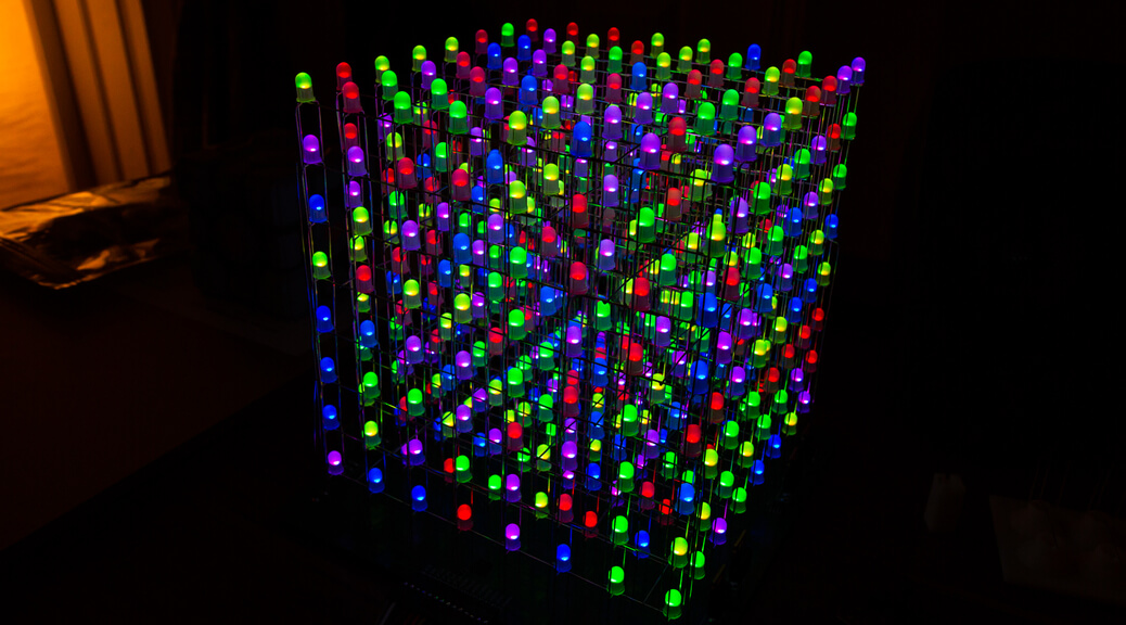
One of the projects that I’ve been working on for the last four months or so is an 8x8x8 RGB LED cube. After looking up some designs online of what others have built, I decided to design and build my own version. Instead of something shoddily put together, I wanted to build a display that could be put outside of one of the introductory lab rooms for other students to program and play around with. Thus, my design had a few goals:
- It had to look professional. This meant that the overall cube should be structurally sound and a proper PCB should be designed for the driving circuitry.
- It had to be fast. Since some sort of multiplexing would be needed to drive 512 LEDs, I wanted the cube to have at least 240Hz* refresh rate at the very minimum.
- It had to be driven from a microcontroller that is used in introductory classes. This meant that it had to be driven from a Digilent Cerebot 32MX7 board that is used to teach microprocessors here at Virginia Tech. While the cube itself isn’t limited to a specific microcontroller, by using this board I can write a baseline for the code from which other students can then easily build off of.
- It had to look impressive.
* – There’s actually a notable difference when driving the cube at 60Hz vs 240Hz.
LED Cube Revision A
With such a large cube, obstructions within the cube must be minimized to allow the LEDs at the back and center to be visible. To achieve this, I designed the first revision of the cube in such a way that no extra wiring was used outside of the leads from the LEDs themselves. This involved bending the leads in four different orientations to allow the layers to stack in such a way that is structurally sound in all directions. To make things easier and more consistent, I 3D printed a few tools to help with bending the leads and trimming them to the correct lengths. The layers were then assembled and soldered by hand with the help of a 3D printed spacer.


")
")
The first revision of the cube was assembled starting from the top layer and working down. Each individual layer took roughly four hours to prepare and solder.


LED Cube Revision B
Since the second revision of the cube was assembled from the bottom up, I decided to make things easier and use only one orientation for each LED. This allowed me to work on batches of LEDs at a time and simplified the workflow. However, using only one orientation for the LEDs meant that I had to use extra wiring to connect up each layer. This ended up adding a bit more metal to the structure but the consistency of the cube made up for the decreased visibility. Once I had enough LEDs for an entire layer, I assembled each layer at a time to test and verify that everything worked up to that point.


")

LED Cube Revision C
For revision C of the design, I wanted to focus on improving the structural stability of the assembled cube. Two changes were made in the design to achieve this. The first was to change it so that each LED piece was more consistent. The problem with the old design was in the plastic pieces used to mold the LED leads into the right shape. It turns out that ABS plastic was more malleable than I had originally thought. This led to the LED leads not being bent at exactly 90 degree angles that I had originally wanted. To fix this, I decided to bend all the leads on the new cube by hand. The second improvement was to increase the surface area between the interconnections of the LEDs. This was done by bending the excess metal inwards, thus providing almost 5 times the surface area for the solder to stick to.
Of course, these changes had some downsides as well. The main problem being that it takes around eight hours to assemble each layer when everything is done by hand. This increase of four hours doubled the time it took to assemble the cube when compared to the previous version. Bending the LEDs by hand also introduced a bit of variation with the lead lengths, which led to difficulties when the layers were soldered together. The upside is that the cube is now structurally sound, enough at least that I’m pretty confident it wont randomly break at the joints. Plus, it looks a lot more consistent when viewed close up.
Within the code base, I also implemented a cube rotation routine as well as a function to overlay an additional frame on top of the base one. This additional overlay is used along with the rotation routine to display scrolling text across the outside of the cube. Unfortunately, I do not have pictures of the scrolling text at this point but I’ll make a note to showcase it when I take a video of it.
With revision C, I’m pretty much done on the hardware side of the cube. My plan at this point is to design and build a good power supply enclosure to move the brick farther away from the cube. I’m also thinking of writing the code base for the microprocessor board to communicate to something like the Electric Imp, which will allow me to send it commands over a wireless network via a web interface.
 vs Rev. C (Right) LED Comparison")
 vs Rev. C (Right) Cube Comparison")
New PSU Design
My goal for the power supply enclosure was to make a well designed transparent enclosure that had adequate cooling and connectivity. The resulting case can be seen below, and I’m pretty satisfied with the result. The case consists of six pieces of laser cut 1/8″ acrylic from pololu.com at about $40. It takes a standard IEC 320-C14 power connector and outputs a DIN-4 cable that has a 3.3, 5, and 15V rail. The other end of this cable can then be connected to the cube, thus turning the cube and PSU into a modular system.
There were three minor issues however with this design. The first problem is that the point where the DIN cable enters the cube is not secured very tightly. This may pose problems if stress is placed upon the cable. Another problem is that the fan that I used is rated for 12V, but the PSU supplies 15V. It works, but the fan runs a bit louder than I would like so I may replace it at a later date. The last issue is with the way that I had designed the laser cut pieces of acrylic. When I was designing the layout of the pieces, I forgot to account for how easily acrylic fractures if proper stress relief is not implemented: I left the corners at a right angle where I should have rounded them instead. This led to some fractures on the corners, but the overall structural stability is largely unaffected.


Component Choice and PCB Design
Major Components List:
- TLC5951 – PWM Driver
- TC4452 – MOSFET Driver
- SN74HC595 – Shift Register
- IRLB8721PBF – MOSFET
- LFVLT150-4102 – Power Supply
- RGB LED (https://www.dipmicro.com/store/LED5AD)
Originally I wanted to use the MAX6975 chip as the PWM driver but after going through the datasheet, I found that it used a framed SPI protocol which I wasn’t sure if the PIC32 microprocessor supported.
The MOSFETs were chosen to switch large of power quickly, with each MOSFET having its own driver to ensure low rise and fall times and thus minimizing power dissipation. Since the MOSFETs were used to source the 5V rail current to the common anode pin for the LEDs, a 15V power rail was required to drive the gate of the MOSFETs. In order to isolate the power source for each rail, a dedicated power supply was chosen that supplied 3.3V, 5V, 15V, and -15V to the board. By isolating the power rails at the power supply, fluctuations within each power rail would be isolated from the other power rails.
Since the TLC5951 chip is designed to sink up to 40mA on each output, up to 8 amps can be sunk through eight chips running at full power. This factored into the power supply choice as the LFVLT150-4102 PSU can supply up to 10A on the 5V rail. This high power usage also factored into the PCB design as well, since attention had to be paid towards properly routing the power rails and isolating them from the signal lines.
A problem with the power supply however, is that the 3.3V and 5V required a minimum load of 0.5A while the 15V and -15V required a minimum load of 0.1A. I used high wattage load resistors to ensure the minimum load requirements were met for each rail, but what I found was that sinking that much current through a load resistor made it difficult to dissipate the heat properly within an enclosure. In fact, one of the load resistors was measured to be 150 degrees Celsius!
")
")
")
")
")
")
Code and Operation of the Cube
The TLC5951 chip has two shift registers, one 27 byte register for the dot correction and global brightness settings (DS) and other being a 36 byte register for the grayscale control (GS). The eight chips that drive the cube are hooked up in series so a total of 216 bytes needs to be written for the DS register and 288 bytes are needed for the GS register. The chip has two SPI input lines, with one for each control register. An interesting feature of the chip however is that only one line is really needed. Keeping the latch input high, data can be clocked into the DS register from the GS line. Aside from the data and latch lines, there also exists a line for the PWM clock that drives the PWM output and an input to tristate the output of the chips. Thus there are seven lines that are used to drive the TLC5951 chip, with a minimum of four lines for slightly slower operation.
In addition to the TLC5951 chip, the shift register is driven by an additional four lines. Combined together, the entire LED cube can be driven by a minimum of eight lines or one and a half PMOD ports on the Cerebot board.
The Cerebot board itself is a just breakout board for the PIC32MX795F512L processor. The processor itself has a 32-bit core running at 80MHz and supports a very large set of peripherals. The library for driving the cube itself is pretty much finished and can be found in my SVN repository under “PIC Stuff/Cerebot_32MX7_LED_Cube/”.
As we can see from the output of the logic analyzer in the pictures below, the entire startup process is shown. Initially the microprocessor writes to the DS register, then waits 7ms before latching in the data. The processor then starts a timer that triggers every 500us to update the display at 250Hz. Once a timer triggers, we can see that sending the data for a single frame (288 bytes) takes about 166.85us. Of that, 64.62us is spent in an interrupt handler. From these values we can calculate that the CPU usage at 250Hz is about 13%. At 60Hz (2083us), the CPU usage goes down to around 3%.
In the frame transmission sequence, the SPI interrupt is triggered every 16 bytes since the SPI FIFO buffer on the processor itself is only 16 bytes deep. If DMA was implemented for the data transfer however, all 288 bytes can be sent with one interrupt so the time spent in an interrupt handler can be reduced by half down to around 30us. This would also cut down the CPU usage down by half as well.
For the current implementation, the SPI module within the processor is set to operate at 20MHz. Since the TLC5951 chip supports up to 30MHz, the timings above can be reduced by an additional 30% if the SPI module was instead configured for 30MHz. The reason why the current code uses 20MHz was because it was an easy divider from the 80MHz that the main processor runs at. If the main processor was overclocked from 80MHz to 90MHz, it would be easy to get the SPI module to run at 30MHz.


Future Improvements
- Find a better power supply that has a lower minimum load requirement
- Replace the SPI implementation in the code with DMA
- Process the returned data from the chip to check the health status of each LED
- Write the code for reading and processing computer generated frame data over USB
Motivation for the Project (extra):
Aside from how I wanted to build a better LED cube in comparison to other projects out there on the Internet, my other reason for building this LED cube is that I wanted to build a flashy impressive display for the AMP Lab. What is the AMP lab you ask? Also known as the Autonomous Mastery Prototyping lab, the AMP lab was established about a year ago here at Virginia Tech to help ECE students get some hands-on experience with building circuit prototypes as well as working on embedded projects. The lab is designed to allow students to be as autonomous as possible, with the main benefits of the lab being the financial support (it’ll buy anything you need for your project) and mentor support (students who have previously completed projects act as mentors for new students). More information on the lab can be found on the lab’s webpage and wiki. (http://www.cel.ece.vt.edu/AMP_Lab/)
One of the majors issues in the lab at the moment is the lack of participation. We don’t have many students working on personal projects since most of the members only join to take the soldering certification course. Thus, there are two other side goals for this project: to get more students to join the lab and to inspire the students currently in the lab to work on projects that they find interesting. Since the AMP lab sits across from the CEL (a support room for undergraduate CPE courses), I figured that a flashy display would be able to attract students who may have their own projects that they want to build. By also using a microprocessor board that is taught in undergraduate courses, students in the AMP lab can use their skills to program the display to show their own animations.
The most common display components out there for beginners consists of single LEDs, strips of LEDs, LCD displays, numeric and character displays, and OLED displays. All of these display types are used to show data, but I feel that there is nothing inherently interesting about these displays. Sure, you can show a string or some numbers on the display, but what else can you do with it? Hence my LED cube. I figured that a 3D display is not only more impressive, but the novelty of the display itself could allow students to think of ways to uniquely utilize this display to do certain things. For example, students can not only program full RGB animations on the cube, but also display scrolling text around the edge of the cube. Games are another possibility: imagine playing 3D snake, pacman, or two player TRON on the cube.


